Fully amorphized source/drain for leaky junctions

a leaky junction and source/drain technology, applied in the field of semiconductor devices, can solve the problems of preventing optimal performance of conventional soi devices, charging often develops within the floating body of the device, and does not have the capability to dissipa

Inactive Publication Date: 2002-05-28
TWITTER INC
View PDF14 Cites 34 Cited by
  • Summary
  • Abstract
  • Description
  • Claims
  • Application Information

AI Technical Summary

Problems solved by technology

For all their advantages, conventional SOI devices have significant drawbacks which prevent them from performing optimally.
As a result, charge often develops within the floating body of the device which does not have the capability to dissipate.
The above approach is undesirable for a number of reasons.
First, it may require use of a separate masking level.
Second, it implants a non-traditional species (Al) that may adversely affect operation of the resulting device.
These approaches involve intentionally creating junction defects in the SOI structure that result in charge leakage into the base.
These conventional methods result in the formation of a source / drain with some "leakiness."

Method used


Image

  • Fully amorphized source/drain for leaky junctions
  • Fully amorphized source/drain for leaky junctions
  • Fully amorphized source/drain for leaky junctions

Examples


Embodiment Construction

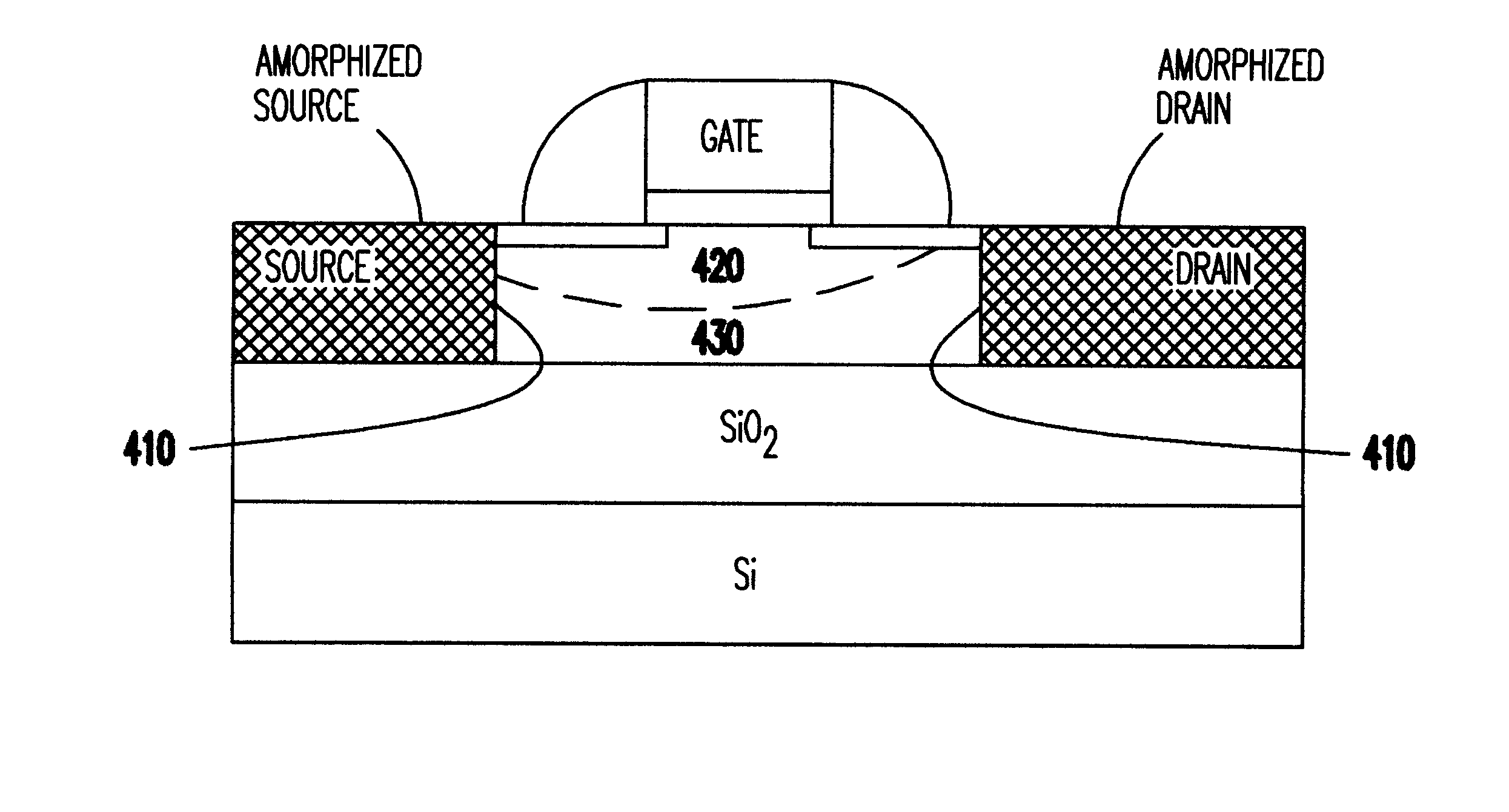
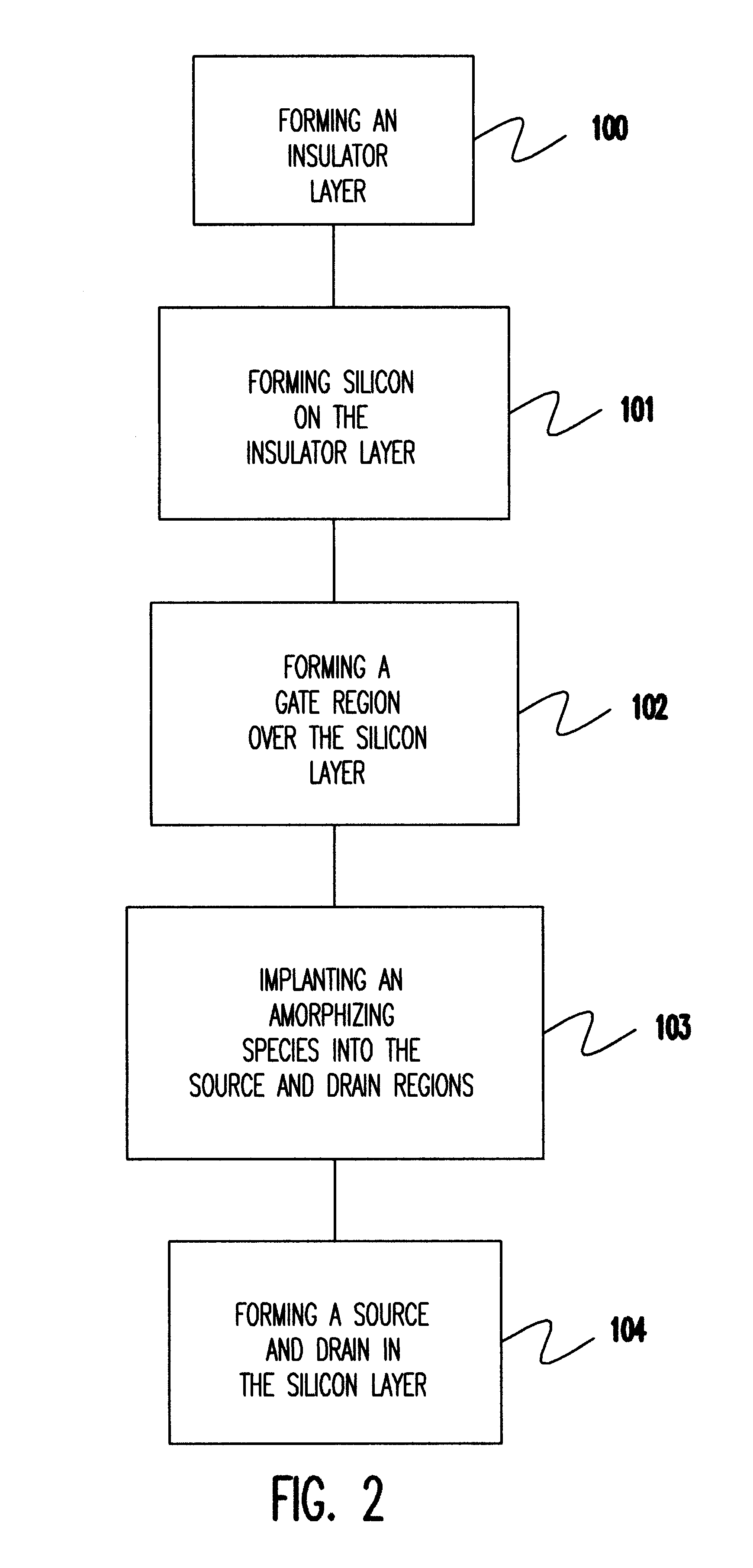
Referring to FIG. 2, the method of the present invention begins by forming SOI semiconductor device which includes a field effect transistor disposed on an insulator layer in accordance with any one of a variety of conventional processing techniques. These techniques may include forming an insulator layer made, for example, of SiO.sub.2, and then forming a silicon layer over the insulator layer. (Blocks 100 and 101). The insulator layer may be formed on a silicon substrate or may have a thickness sufficient to effectively serve as the substrate itself. Additional masking and deposition steps are then performed to create the gate region at a position over top the channel in the silicon (Block 103).

Once these elements are formed, the method continues by implanting an amorphizing species into the source region and the drain region of the silicon layer. (Block 103). The concentration and depth of implantation are sufficient to ensure that the source and drain regions are fully amorphize...


PUM


Abstract

A semiconductor device having a silicon-on-insulator (SOI) structure includes a field-effect transistor having amorphized source and drain regions formed by implanting silicon or germanium ions into a silicon layer formed over a buried insulator. The fully amorphized source and drain regions ultimately result in permanent crystalline defects that cause p-n junction leakage which allows charge in the body of the device to dissipate, thereby improving the overall efficiency and performance of the device. The source and drain regions are amorphized throughout their entire thickness to prevent single crystal re-crystallization from occurring during annealing and other subsequent processing steps that can degrade the quality of the p-n leakage junctions.

Description

1. Field of the InventionThe present invention generally relates to semiconductor devices, and more particularly to semiconductor devices having a silicon-on-insulator structure that dissipates charge within the floating body of the device.2. Background DescriptionSemiconductor devices with a silicon-on-insulator (SOI) structure have an insulator layer buried under a thinner silicon layer that typically contains the source and drain regions of one or more field-effect transistors. SOI devices, more specifically, may be categorized as having one of two basic structures. The first structure includes a thin layer of silicon, usually 0.5 .mu.m or less, on top of a thick insulator layer, which serves as the entire substrate for the device. Silicon-on-sapphire devices exemplify this type of SOI. The second structure includes an insulator layer sandwiched between a silicon substrate and an overlying silicon layer. Separation by implanted oxygen (SIMOX) devices and those made by wafer bondi...

Claims


Application Information

Patent Timeline
Patent Type & Authority Patents(United States)
IPC IPC(8): H01L21/02H01L29/786H01L21/265H01L21/336H01L29/66H01L29/78
CPCH01L21/26506H01L29/66772H01L29/78621H01L29/78612H01L29/78618H01L29/78609H01L29/78
Inventor CROWDER, SCOTTSCHEPIS, DOMINIC J.SHERONY, MELANIE J.
Owner TWITTER INC
Why Eureka
Try Eureka