Semiconductor device having micro-wires designed for reduced capacitive coupling

a technology of capacitive coupling and micro-wires, which is applied in the direction of semiconductor devices, semiconductor/solid-state device details, electrical apparatus, etc., can solve the problems of narrow space between adjacent micro-wires and increase the area of adjacent side portions of micro-wires, so as to increase the surface area of wiring without increasing capacitance

Inactive Publication Date: 2002-06-04
NEC ELECTRONICS CORP
View PDF6 Cites 18 Cited by
  • Summary
  • Abstract
  • Description
  • Claims
  • Application Information

AI Technical Summary

Benefits of technology

In short, for attaining the above object, the present invention is based on a wiring structure (i.e., cross sectional shape) that increases the surface area of wiring without increasing the capacitance between adjacent micro-wires by providing a cross-sectional shape of micro-wires whose side portion is partially open (or recessed or bored).

Problems solved by technology

However, this makes the space between adjacent micro-wires narrow and the area of the adjacent side portions of micro-wires is increased.

Method used


Image

  • Semiconductor device having micro-wires designed for reduced capacitive coupling
  • Semiconductor device having micro-wires designed for reduced capacitive coupling
  • Semiconductor device having micro-wires designed for reduced capacitive coupling

Examples


Embodiment Construction

The present invention is explained in more detail below by describing specific examples with reference to the annexed drawings.

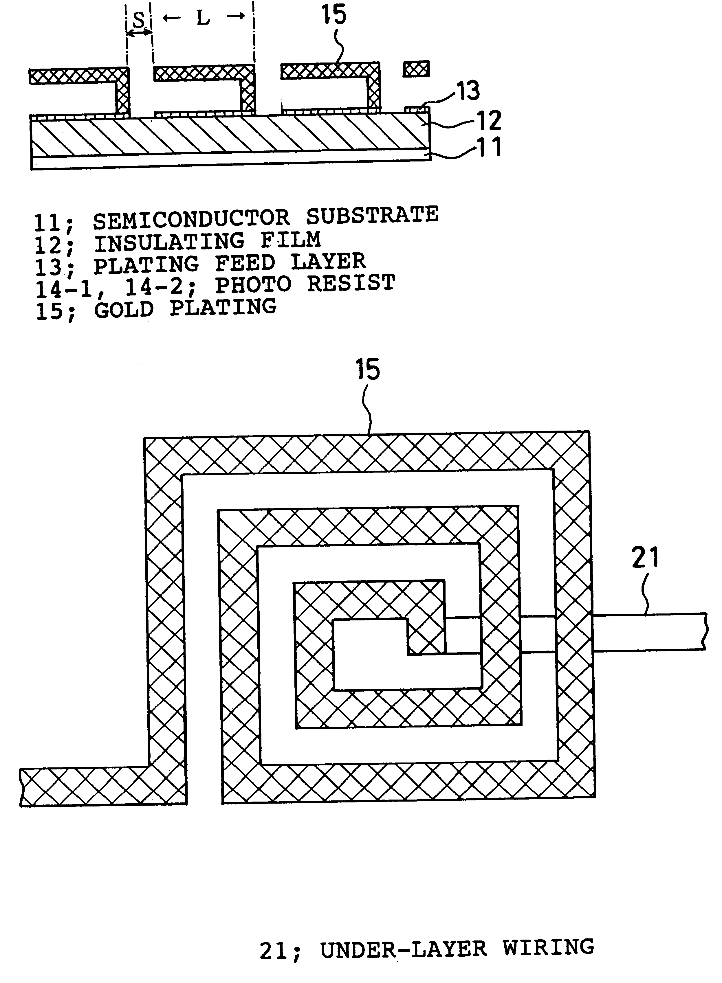
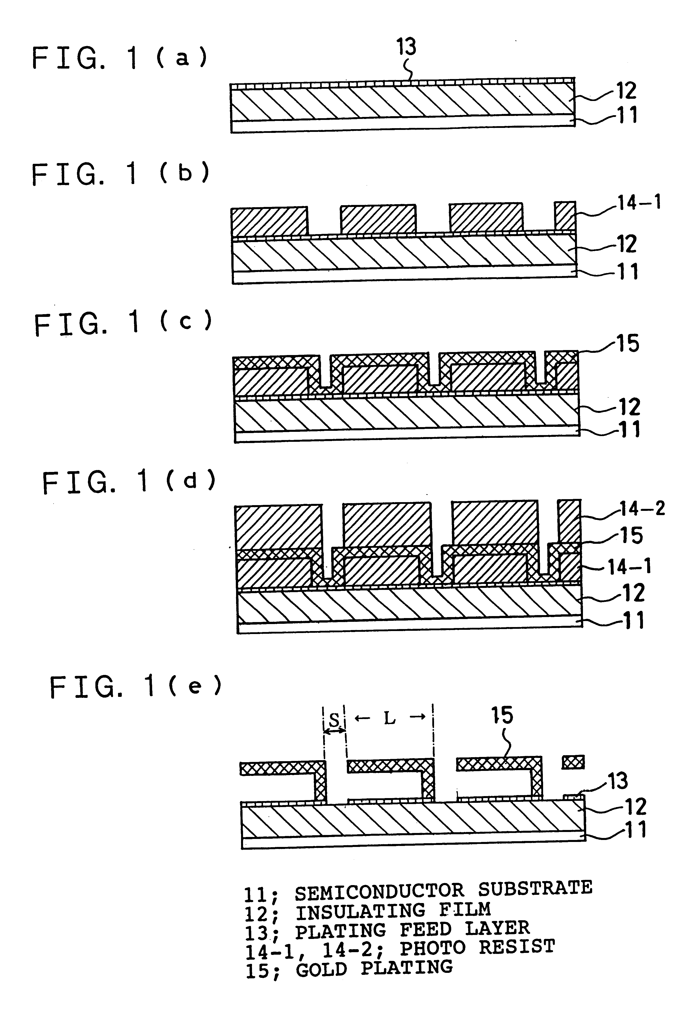
FIG. 1 shows a cross-sectional view showing a first example of the semiconductor device of the present invention in the order of its preparation steps.

At first, a plating feed layer 13 is formed on an insulating film 12 laid on a semiconductor substrate 11 by sputtering or other method (see FIG. 1 (a)).

Next, on the plating feed layer 13, photoresist 14-1 is coated and then exposed and developed in accordance with usual lithographic technology to form a predetermined pattern (see FIG. 1 (b)).

Then, a plating feed layer 13 is applied by spattering etc. and a gold plating 15 of around 300 nm thick is applied using electro- or electroless-plating etc. to form a wiring portion (see FIG. 1(c)).

Subsequently, on the resultant gold plating 15, photoresist 14-2 is coated and then exposed and developed in accordance with usual lithographic technology to form a predeterm...


PUM


Abstract

Semiconductor device in which wiring surface area is increased while the increase of the capacitance between adjacent micro-wires is inhibited. The device can be prepared by forming an insulating layer and a plating feed layer in this order on a semiconductor substrate, plating after masking the plating feed layer with a first photoresist to form a gold plating, etching off the gold plating and the plating feed layer except for a wiring portion by dry-etching after masking the resultant surface with a second photoresist, removing then the first and second photoresists to form micro-wires, in which the same direction of the side portion is opened. The cross section may be U-shape arranged with U being turned sideways.

Description

This invention relates to a semiconductor device, more especially to a semiconductor device comprising micro-wires of a preferable shape for use in a high-frequency semiconductor device.Recently, progress has been made in the development of a high-frequency integrated semiconductor such as GaAs integrated semiconductors which operate over a wide range of frequencies, spanning from a few GHz to 100 GHz. Wiring within these semiconductors is accomplished using microstrip lines. Transmission loss of signals traveling in the microstrip lines is a problem caused by increased resistance due to skin effect accompanied by the use of high frequency signals.In order to reduce the increased of resistance due to skin effect, increasing the surface area of wiring is considered effective and a variety of processes for increasing the surface area of wiring have been hitherto known.These examples include a process for increasing the film thickness of wiring as shown in FIG. 4(b) and a process for i...

Claims


Application Information

Patent Timeline
Patent Type & Authority Patents(United States)
IPC IPC(8): H01L23/522H01L23/52H01L21/822H01L21/3205H01L27/04
CPCH01L23/5222H01L23/5227H01L2924/0002H01L2924/00H01L27/04
Inventor TAKAHASHI, KIYOSHI
Owner NEC ELECTRONICS CORP
Why Eureka
Try Eureka