Semiconductor device

a technology of semiconductor devices and semiconductor components, applied in semiconductor devices, semiconductor/solid-state device details, electrical devices, etc., can solve the problems of insufficient bonding between the connecting part of the chip and the substrate, damage to the semiconductor device, and bad effect on the reliability of the semiconductor devi

Inactive Publication Date: 2002-06-04
RENESAS ELECTRONICS CORP
View PDF7 Cites 20 Cited by
  • Summary
  • Abstract
  • Description
  • Claims
  • Application Information

AI Technical Summary

Problems solved by technology

If there is a void (a part in which the bubble is present) in the resin 6 when the semiconductor device is heated to become a high temperature, then inside air is expanded to explode the bubble, resulting in a damage of the semiconductor device.
However, a temperature condition in manufacturing steps sometimes caused a bad effect on a reliability of the semiconductor device.
In the case of a low temperature in flip chip connection, the connecting part between the chip and the substrate has been insufficiently bonded to lower the reliability.
Contrarily, in the case of a high temperature, the semiconductor chip may be deteriorated.
In the case of using a glass epoxy substrate for the substrate 15, a low heat-resistant temperature thereof does not allow other choice than a material such as a solder or the like, which can be bonded at a relatively low temperature.
However, using solder bumps is easy to cause a short circuit.
As measures for this defect, respective pads have to be arranged with a certain distance, causing difficulties in making a fine pitch.
However, the conventional semiconductor device using the film substrate as shown in FIG. 1 has an adhesive layer 10a, resulting in insufficient heat resistance.
In addition, also having the adhesive layer 10a causes sinking of the connecting part by applying a high pressure in thermocompression bonding to lower the reliability of the connection.
There is another structural problem in the conventional semiconductor device such that the substrate structure becomes complicated because of through holes.
As a result, the semiconductor device becomes costly.
For example, it is very difficult to perfectly prevent the mixing of air bubbles into the sealing resin because of a microscopic step formed at a boundary region between the substrate and the wiring layer.

Method used


Image

  • Semiconductor device
  • Semiconductor device
  • Semiconductor device

Examples


Embodiment Construction

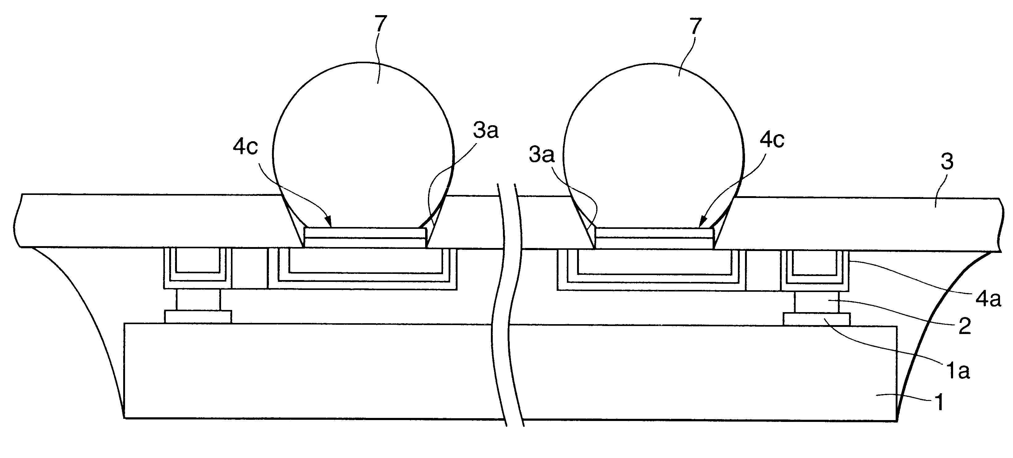
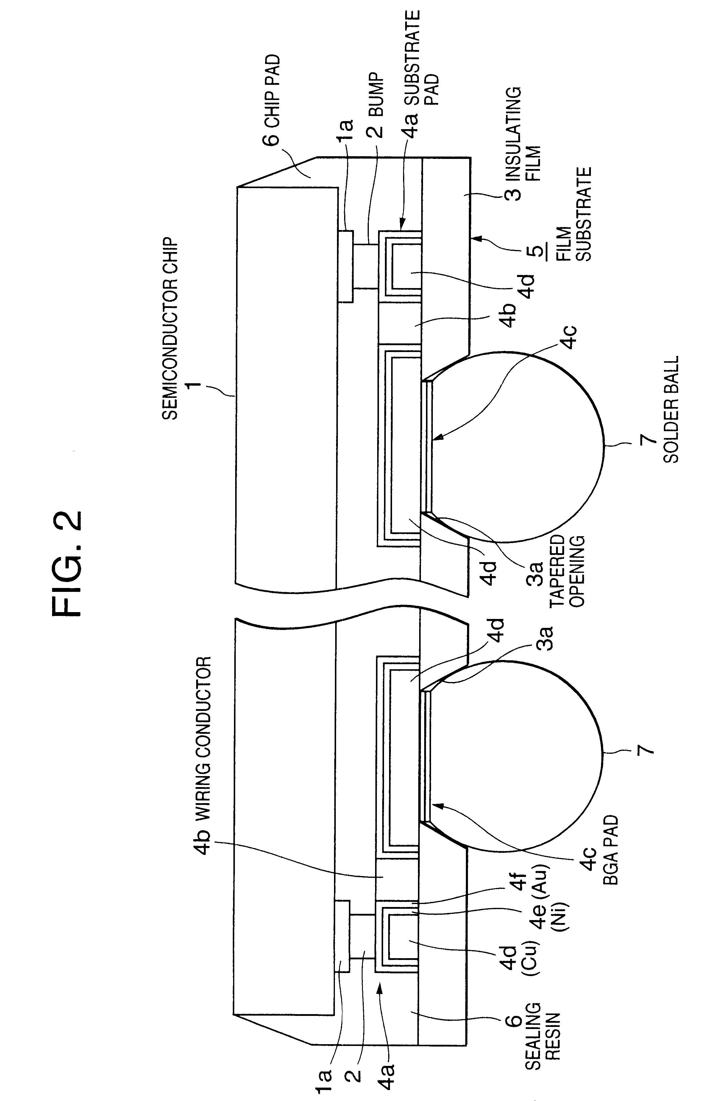
The practical sizes of respective parts of the semiconductor device of the present embodiment will be illustrated below. The size of the semiconductor chip 1 is 7.times.14.times.0.3 mm. An Au bump 2 having a diameter of 100 .mu.m and a height of 30 .mu.m is formed on a corresponding chip pad 1a of the semiconductor chip 1 by ball bonding.

The size of a chip pad la and a substrate pad 4a is 90 .mu.m square. The chip pad 1a has an area of 59 pins and the minimum pitch thereof is 120 .mu.m.

The polyimide film 3 used in the film substrate 5 is 50 .mu.m thick. The wiring layer is mainly made of copper (Cu) and may be formed directly on one face of the polyimide film 3 by electrolytic plating. There Is no adhesive layer between the polyimide film 3 and the wiring layer. Therefore, the wiring layer is excellent for heat resistance and also high in rigidity in a direction of thickness as a whole.

More specifically, the wiring layer (the substrate pads 4a, the wiring conductors 4b and the BGA p...


PUM


Abstract

A semiconductor device allowing a finer terminal pitch, a low profile, and easy product inspection is disclosed. A semiconductor device includes a semiconductor chip and a film substrate having the semiconductor chip connected thereon. The film substrate includes an insulating film having a plurality of openings formed in a desired pattern and a wiring layer formed in a chip-connecting surface of the insulating film. Solder balls are each directly bonded to the external connection pads through the openings. The wiring layer includes substrate pads each being connected to the chip pads of the semiconductor chip, and external connection pads each being electrically connected to these substrate pads. The external connection pads are each formed over the openings so that the openings are covered with the external connection pads on the chip-connecting surface of the insulating film, respectively.

Description

1. Field of the InventionThe present invention relates to a semiconductor device manufactured by using a flip chip connection to form external connection terminals.2. Description of the Prior ArtThere has been disclosed a semiconductor device manufactured by using a flip chip connection method in Japanese Patent Application Unexamined Publication No. 8-279571.FIG. 1 shows an example of such a conventional semiconductor device. In FIG. 1, a semiconductor chip 1 is mounted on a substrate 15 through metal bumps 9 for connection. For a substrate material, a ceramic, a glass epoxy resin, or a plastic film may be used. Here, the substrate 15 is composed of a thin, flexible plastic film 10 having pads 11 and wiring conductors 12 formed on the top surface thereof through an adhesive layer 10a and having BGA (Ball Grid Array) pads 14 formed on the bottom surface thereof. A pad 11 and the corresponding wiring conductor 12 are electrically connected to the corresponding BGA pad by a through ho...

Claims


Application Information

Patent Timeline
Patent Type & Authority Patents(United States)
IPC IPC(8): H01L23/31H01L23/28H01L23/48H01L23/498H01L23/552H01L23/12
CPCH01L23/3114H01L23/49838H01L23/4985H01L23/552H01L23/49816H01L2924/01322H01L2224/1134H01L2224/131H01L2224/13144H01L2224/16237H01L2924/01057H01L2924/01078H01L2924/01079H01L2924/09701H01L2924/15183H01L2924/15184H01L2924/15311H01L2924/3025H01L2224/73204H01L2224/32225H01L2224/16225H01L2924/00013H01L2924/014H01L2924/00014H01L2224/13099H01L2924/00H01L2224/05568H01L2224/05573H01L2224/05624H01L2224/05647H01L23/48
Inventor KIMURA, TAKEHIROISOZAKI, SEIYA
Owner RENESAS ELECTRONICS CORP
Why Eureka
Try Eureka