Methods of fabricating a memory device

a memory device and memory technology, applied in the field of semiconductor processing, can solve the problems of reducing the available wafer area of devices, unable to maintain or even increase the capacitance of devices while minimum geometries continue to shrink, and unable to grow hsg with sufficient surface area

Inactive Publication Date: 2002-06-11
SAMSUNG AUSTIN SEMICON
View PDF72 Cites 10 Cited by
  • Summary
  • Abstract
  • Description
  • Claims
  • Application Information

AI Technical Summary

Problems solved by technology

Device scaling in integrated circuit design has produced an attendant decrease in the available wafer areas for devices, such as dynamic random access memory cells ("DRAMs").
Because the capacitance of a memory cell capacitor is proportional to the surface area of the capacitor electrodes, the job of maintaining or even increasing device capacitance while minimum geometries continue to shrink is difficult.
The HSG may not grow with sufficient surface area if the dopant concentration of the capacitor electrode exceeds certain levels.
However, manufacturing experience has demonstrated that a physical mechanism associated with the conventional phosphorus anneal is limiting phosphorus diffusion into the silicon electrode.
As a result, the conventional phosphorus doping anneal following HSG silicon growth may not yield desired doping levels.

Method used


Image

  • Methods of fabricating a memory device
  • Methods of fabricating a memory device
  • Methods of fabricating a memory device

Examples


Embodiment Construction

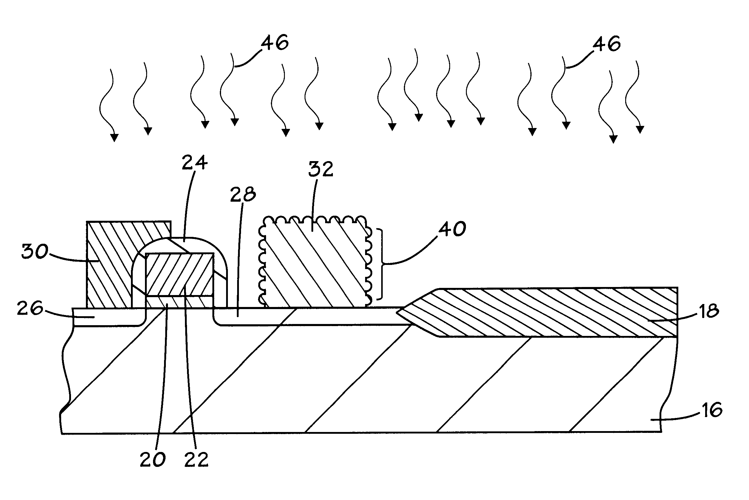
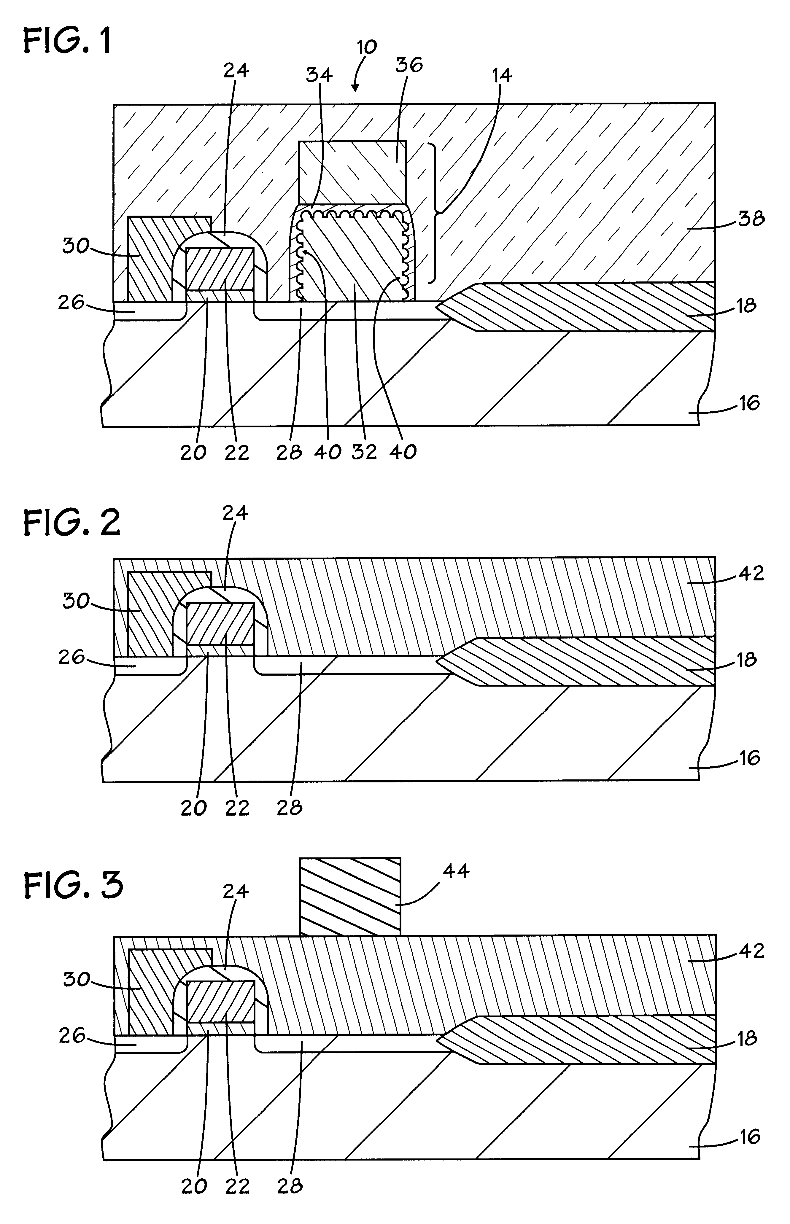
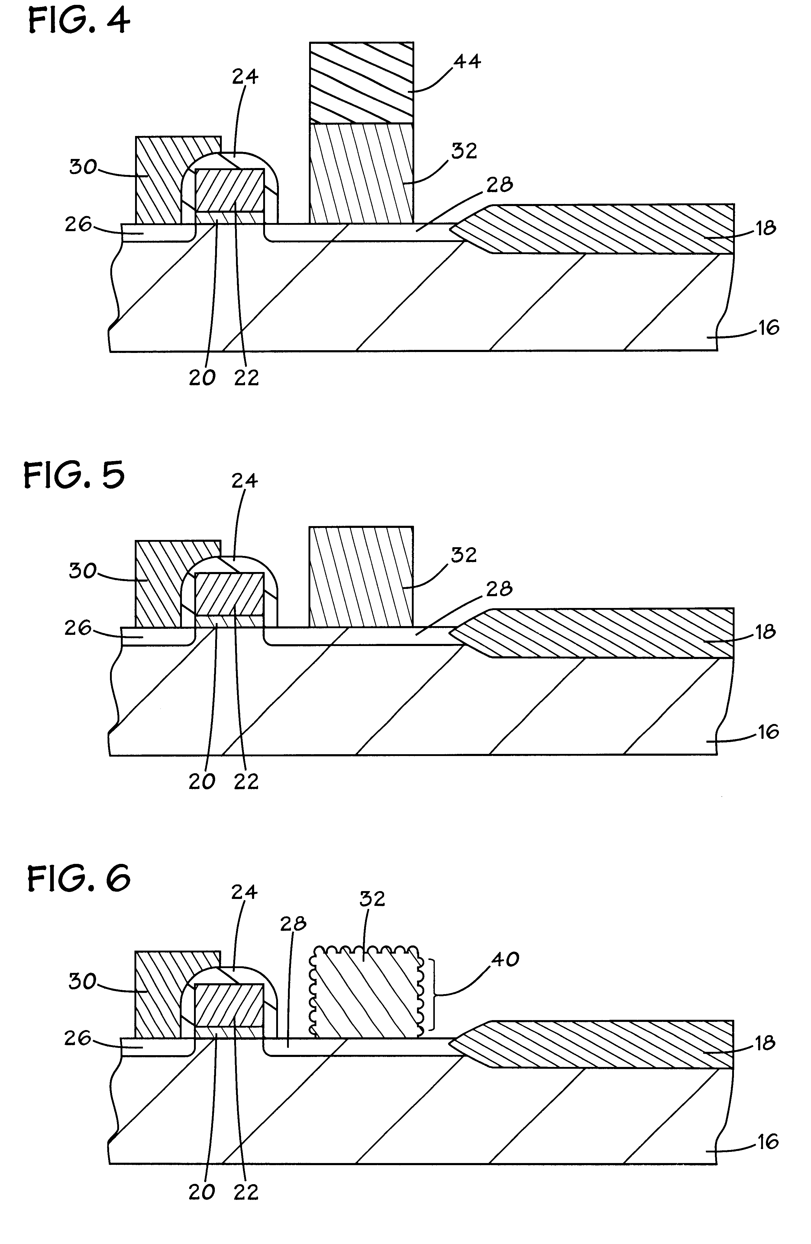
In the drawings described below, reference numerals are generally repeated where identical elements appear in more than one figure. FIG. 1 is a simplified cross-sectional view of an exemplary embodiment of a memory cell 10 that includes an access transistor 12 and a capacitor 14 formed on semiconductor substrate 16. The memory cell 10 is electrically isolated laterally by field oxide regions, one of which is shown and designated 18 for simplicity of illustration. The substrate 16 may be composed of n-type silicon, p-type silicon, silicon-on-insulator or other suitable substrate materials. The access transistor 12 includes a gate dielectric layer 20 formed on the substrate 16, a gate electrode 22 positioned on the gate dielectric layer 20 and a blanket insulating film 24 covering the gate dielectric layer 20 and the gate electrode 22. Source / drain regions 26 and 28 are formed in the substrate. A bit line 30 is positioned in contact with the source / drain region 26.

The storage capacito...


PUM

PropertyMeasurementUnit
temperatureaaaaaaaaaa
thicknessaaaaaaaaaa
pressureaaaaaaaaaa

Abstract

Various methods of fabricating circuit devices are provided. In one aspect, a method of fabricating a circuit device on a substrate is provided. The method includes forming a doped silicon structure on the substrate and forming a hemispherical grain silicon film on the silicon structure. The substrate is heated from a first temperature to a second temperature while undergoing exposure to a dopant gas to add a dopant to the hemispherical grain silicon film. The method provides for improved capacitor electrode fabrication via concurrent gas exposure and substrate temperature ramp-up. In this way, dopant gas is introduced before the doped silicon structure transitions from an amorphous state to a polycrystalline state.

Description

1. Field of the InventionThis invention relates generally to semiconductor processing, and more particularly to methods of fabricating memory devices, such as a capacitor electrodes, utilizing doping anneals.2. Description of the Related ArtDevice scaling in integrated circuit design has produced an attendant decrease in the available wafer areas for devices, such as dynamic random access memory cells ("DRAMs"). As a consequence, memory cell capacitors must be squeezed into ever shrinking spaces. Because the capacitance of a memory cell capacitor is proportional to the surface area of the capacitor electrodes, the job of maintaining or even increasing device capacitance while minimum geometries continue to shrink is difficult. Because DRAM memory cell operation typically improves with increased capacitance, a variety of methods have been developed in an attempt to increase storage electrode surface areas while at the same time maintaining or reducing wafer area taken up by a memory ...

Claims


Application Information

Patent Timeline
Patent Type & Authority Patents(United States)
IPC IPC(8): H01L21/02H01L27/108H01L21/8242
CPCH01L28/84H10B12/00
Inventor EL-HAMDI, MOHAMEDSAWAYA, SAM E.BALFOUR, SCOTTSEMAAN, LOUAY M.
Owner SAMSUNG AUSTIN SEMICON
Why Eureka
Try Eureka