

Oscillation circuit, electronic circuit using the same, and semiconductor device, electronic equipment, and timepiece using the same
a technology of oscillating circuits and circuits, applied in the field of oscillating circuits, electronic circuit semiconductor devices, electronic equipment, and timepieces using the same, can solve problems such as power consumption of the entire circui
- Summary
- Abstract
- Description
- Claims
- Application Information
AI Technical Summary
Benefits of technology
Problems solved by technology
Method used
Image

Examples
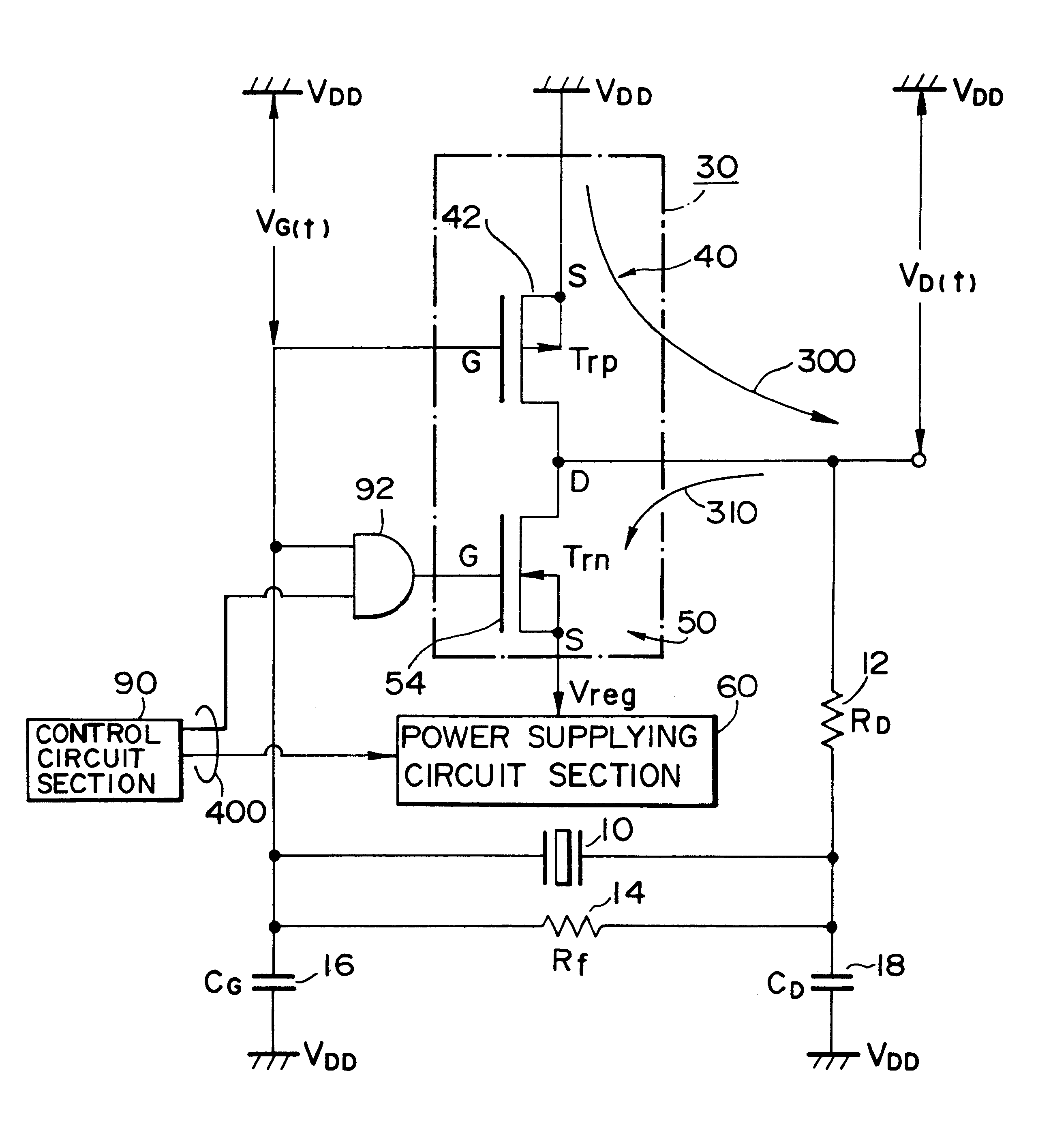
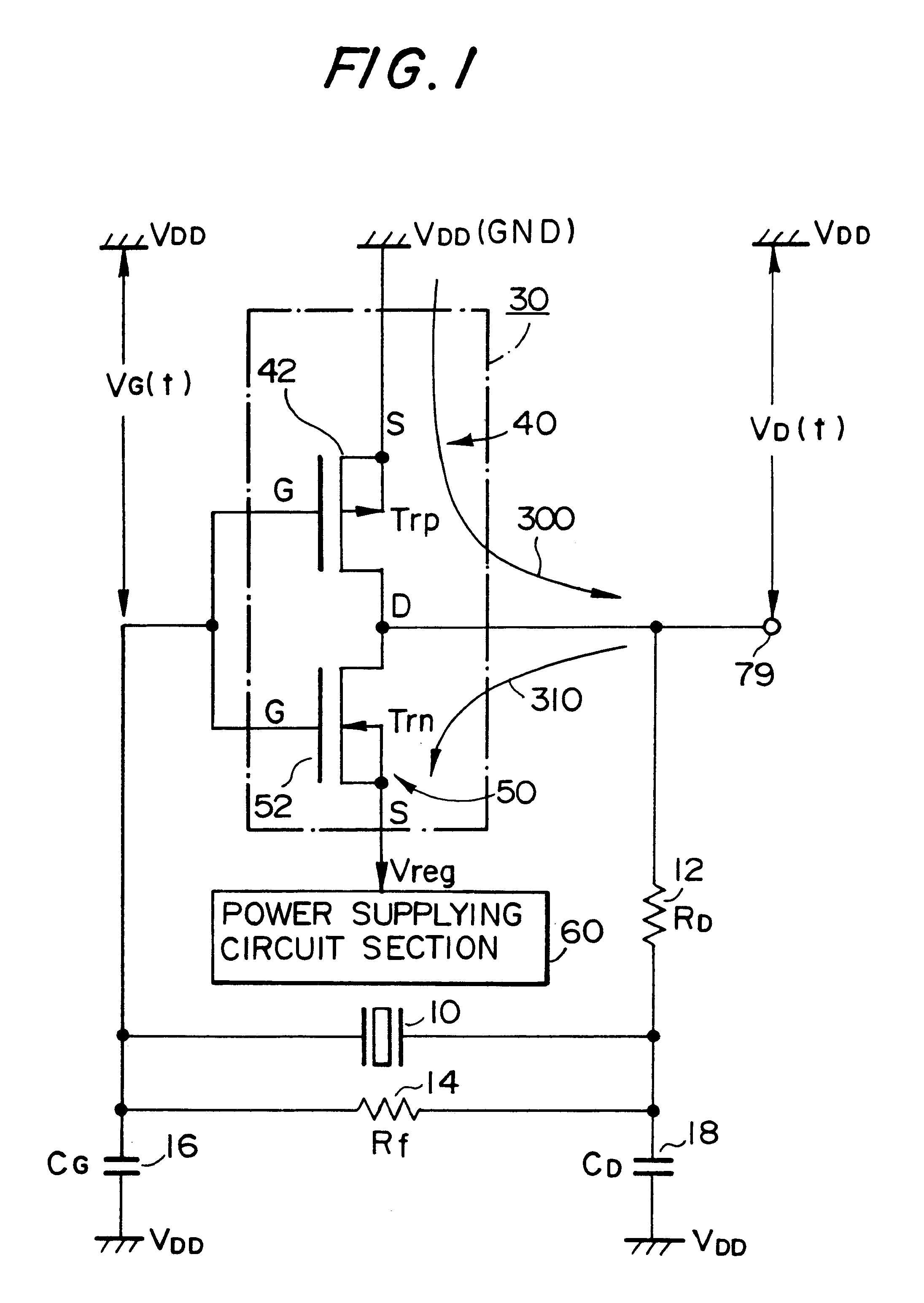
first embodiment
(Modified Form of First Embodiment)
In order to further reduce the power consumption and satisfy the following formulae, the threshold voltages V.sub.TP and V.sub.TN of the transistors 42 and 52 should not be reduced. The constant voltage V.sub.reg should be reduced to its lower limit.
.vertline.V.sub.reg.vertline..ltoreq..vertline.V.sub. TP.vertline.+.vertline.V.sub.TN.vertline. (2)
.vertline.V.sub.reg.vertline.>.vertline.V.sub.TP.vertline., V.sub.reg.vertline.>.vertline.V.sub.TN.vertline. (3)
In other words, as shown in FIG. 19, the drain current I.sub.D at the sub-threshold region 1100 increases exponentially when the threshold voltage decreases as it is apparent from the formula (c). Therefore, it is undesirable to reduce the threshold voltage.
FIGS. 20 and 21 show the changes in only the V.sub.reg. The relationship between V.sub.reg1 and V.sub.reg2 in FIGS. 20 and 21 is .vertline.V.sub.reg1.vertline.>.vertline.V.sub.reg2.vertline.. (The threshold voltage is the same in FIGS. 20 and ...
second embodiment
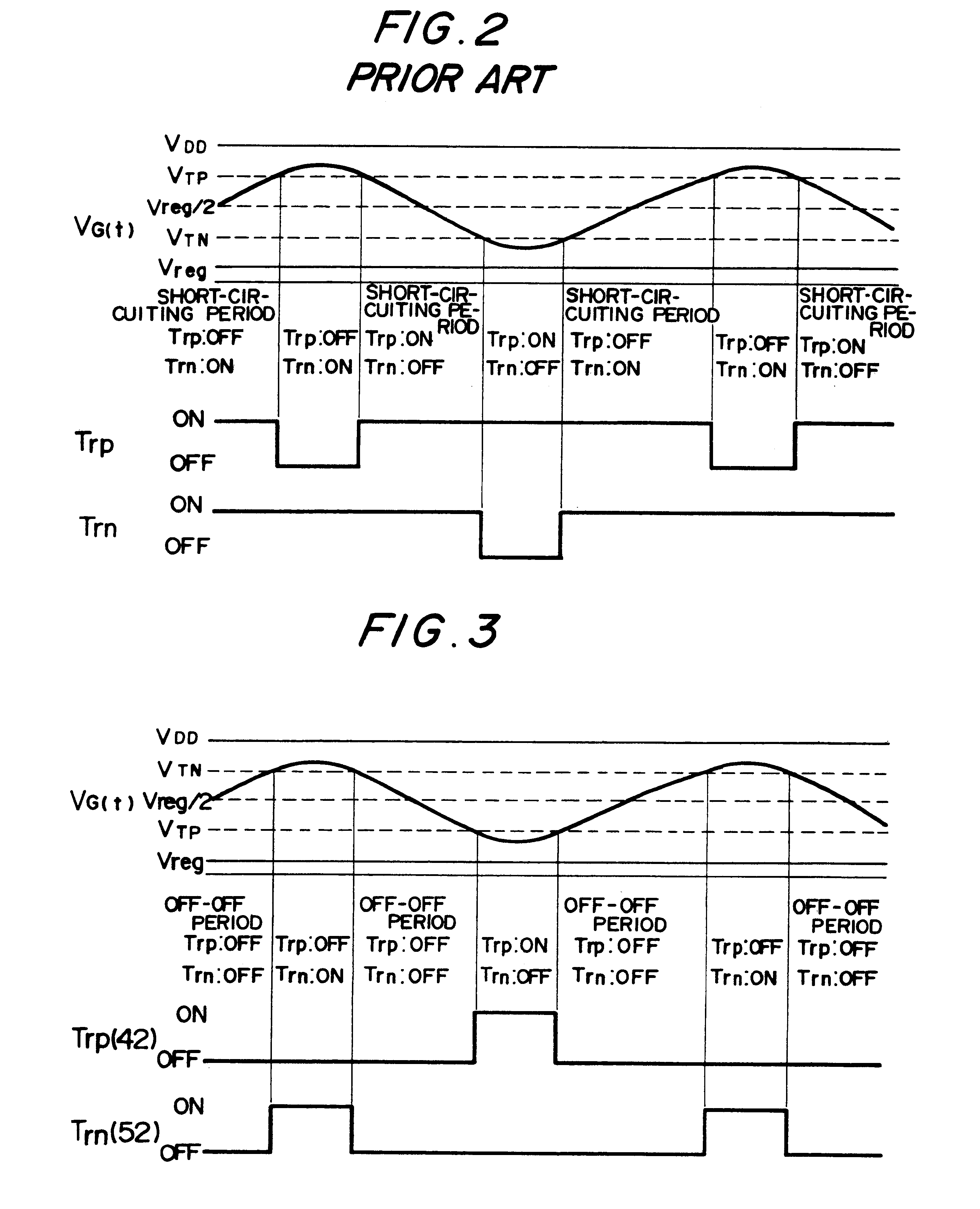
The first embodiment was described above as being configured in such a manner that the threshold voltages of the transistors 42 and 52 satisfied Equation (2) to reduce the short-circuiting current, by way of example. This second embodiment of the invention makes it possible to reduce the short-circuiting current of the inverting amplifier 30 in a manner similar to that of the first embodiment, by applying direct current (DC) bias voltages to the gates of the transistors 42 and 52, even when those transistors 42 and 52 are configured to satisfy the condition of Equation (1), as in the prior art.
The crystal oscillation circuit of this embodiment is shown in FIG. 7 and a timing chart thereof is shown in FIG. 8.
This crystal oscillation circuit comprises a first bias circuit 70 and a second bias circuit 80 that each cause a shift in the DC potential of the feedback input V.sub.G(t) of the inverting amplifier 30 that is input to the gates of the transistors 42 and 52.
These bias circuits 7...
PUM
 Abstract
Description
Claims
Application Information