Structure of solder bumps with improved coplanarity and method of forming solder bumps with improved coplanarity

a technology of coplanarity and solder bumps, which is applied in the direction of soldering apparatus, semiconductor/solid-state device details, manufacturing tools, etc., can solve the problems of uneven distribution of plating current density across the wafer, hard to electroplate solder bumps of uniform height all the way across the wafer, and uneven plating bump height. , to achieve the effect of improving coplanarity

Inactive Publication Date: 2002-07-09
SILICONWARE PRECISION IND CO LTD
View PDF21 Cites 78 Cited by
  • Summary
  • Abstract
  • Description
  • Claims
  • Application Information

AI Technical Summary

Benefits of technology

FIGS. 3A and 3B are a method of forming solder bumps on a UBM structure with improved coplanarity in accordance with a second preferred embodiment of the present invention.

Problems solved by technology

However, it is hard to electroplate solder bumps of uniform height all the way across a wafer.
One problem with electroplating that contributes to solder bumps being formed at a non-uniform height is the uneven distribution of plating current density across a wafer.
When the solder bumps having various heights across a wafer, there will be difficulty in the bonding process and the efficiency, reliability and yield of the production will be affected due to the reworked or scraped chips.
If the bonding pad is damaged, the device will be affected.
Different heights of the solder bumps cause bad bonding between chips to a package carriers, and bad connections will also affect the device functions even damaging the devices.

Method used


Image

  • Structure of solder bumps with improved coplanarity and method of forming solder bumps with improved coplanarity
  • Structure of solder bumps with improved coplanarity and method of forming solder bumps with improved coplanarity
  • Structure of solder bumps with improved coplanarity and method of forming solder bumps with improved coplanarity

Examples


first embodiment

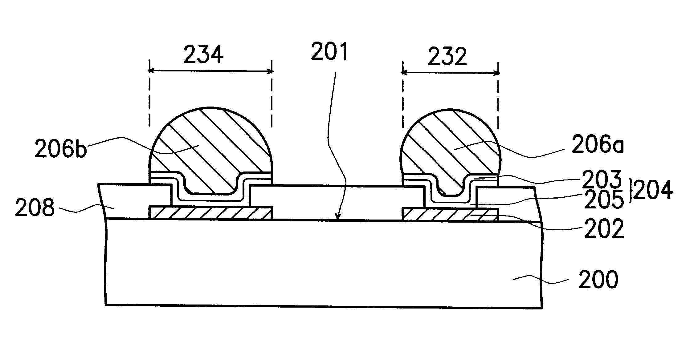
The present invention provides an under bump metal (UBM) structure of solder bumps with improved coplanarity. The UBM structure of the preferred embodiment of the present invention comprises various sizes of areas in order to control the height of solder bumps.

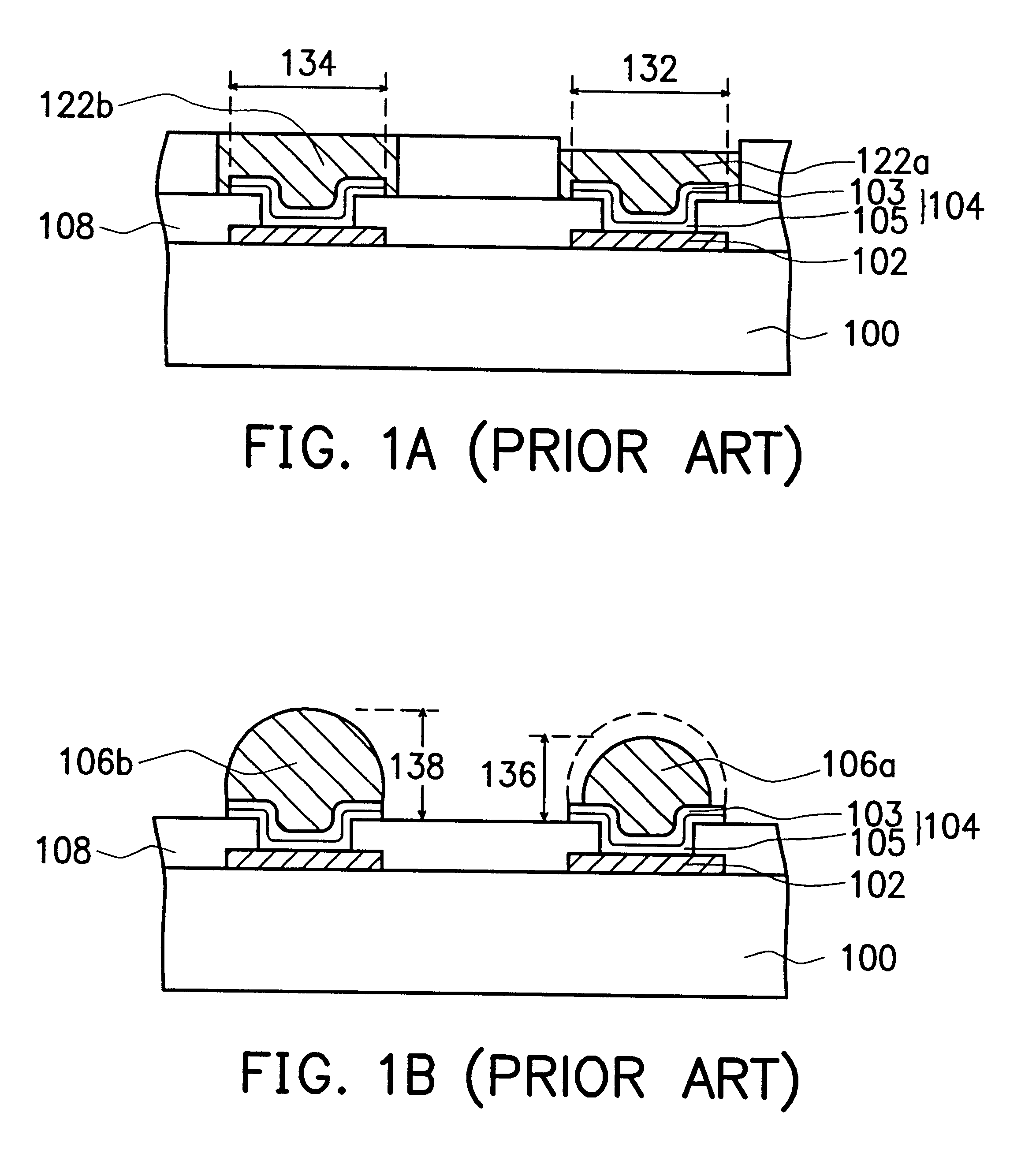
The process of forming the solder bumps begins after bonding pads have been formed on the top surface of the semiconductor wafer. In one known technique, after the bonding pads have been formed, an UBM layer is deposited on top of the semiconductor wafer (including the bonding pads) and covered with a photoresist layer. The UBM layer is placed on top of the semiconductor wafer because the solder material that is used to form the solder bumps does not readily adhere to the bonding pads. The protective layer of photoresist is then patterned and removed in the areas above the bonding pads utilizing known photolithographic processes. Removing portions of the photoresist in the areas above the contact pads exposes the UBM layer tha...

second embodiment

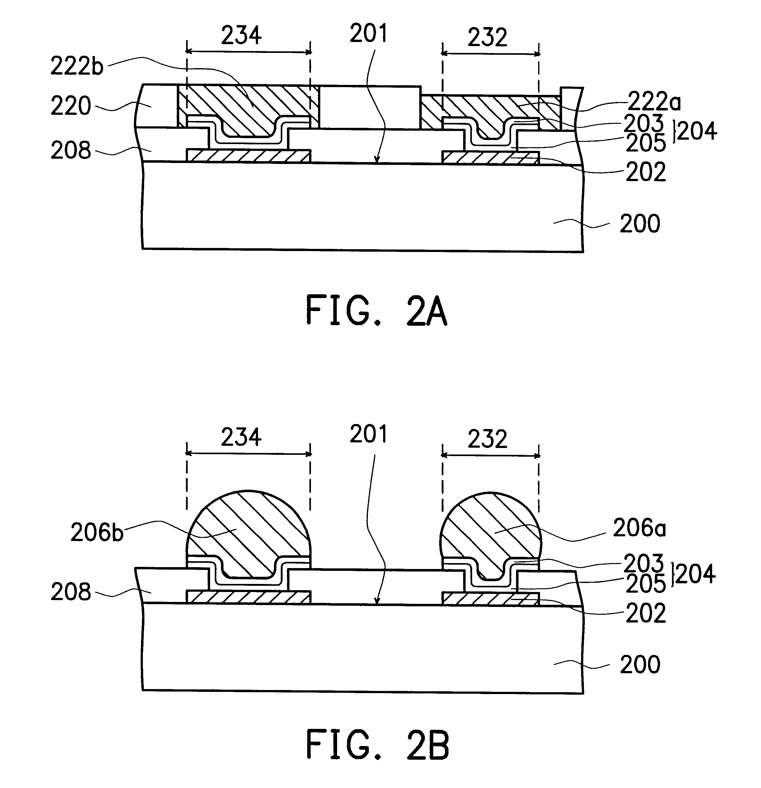
The present invention provides a method of forming solder bumps with improved coplanarity. FIGS. 3A and 3B illustrate a method of forming solder bumps on a UBM structure with improved coplanarity in accordance with a second preferred embodiment of the present invention.

Referring to FIG. 3A, a substrate 300 comprises at least one active surface 301, wherein a plurality of bonding pads 302 that formed on the active surface 301 are serving as connecting nodes to external circuits. The bonding pads 302 are made of aluminum, for example. A passivation layer 308 is formed over the active surface 301, wherein portions of the bonding pads are exposed by the passivation layer 308. The passivation layer 308 can be a polyimide layer but is preferably a silicon oxide layer, silicon nitride layer or layers of other passivation materials known to those having skill in the art. A plurality of UBM layers 304 are formed on the exposed portions of bonding pads 302. The UBM layers 304 have various ope...


PUM

PropertyMeasurementUnit
areaaaaaaaaaaa
sizesaaaaaaaaaa
heightaaaaaaaaaa

Abstract

A structure of solder bumps with improved coplanarility, comprising a substrate, a passivation layer, a plurality of Under Ball Metallurgy (UBM) layers and a plurality of solder bumps. The substrate has at least an active surface, and a plurality of bonding pads are provided thereon. The UBM layers with various areas are electrically connected to the bonding pads. Finally, the solder bumps are formed with uniform-height on the UBM layers. A method of forming solder bumps with improved coplanarity. A UBM structure with various sizes of openings is provided to control the volume of the solder, wherein the various sizes of openings are corresponding to the current distribution across the wafer. The purpose of the various openings is to control the volume of the solder in order to form uniform-heights of solder bumps, the coplanarity of the solder bumps can thus be improved.

Description

This application claims the priority benefit of Taiwan application serial no. 89115393, filed Aug. 01, 2000.1. Field of the InventionThe present invention relates generally to semiconductor device fabrication, and more particularly, to a structure of solder bumps with improved coplanarity and a method of forming solder bumps with improved coplanarity.2. Description of the Related ArtWith recent advances in semiconductor fabrication technology and the increasing demand for improving connection density of semiconductor applications, various techniques have been developed for having a large number of input / out points (I / Os) in a device. The flip-chip technology is being utilized to allow more I / Os on an integrated circuit device.In the packaging industry, the flip-chip packaging can reduce inductance while providing a higher interconnection density and ultimately, a lower cost. The flip-chip technique utilizes solder bumps instead of wires to connect bonding pads on an integrated circu...

Claims


Application Information

Patent Timeline
Patent Type & Authority Patents(United States)
IPC IPC(8): H01L21/02H01L21/60H05K3/34
CPCH01L24/03H01L24/05H01L24/11H01L2224/0401H01L2224/05599H01L2224/1147H01L2224/13099H01L2224/131H01L2924/01013H01L2924/01014H01L2924/01022H01L2924/01028H01L2924/01029H01L2924/01046H01L2924/01047H01L2924/0105H01L2924/01074H01L2924/01078H01L2924/01079H01L2924/01082H01L2924/014H01L2924/05042H01L2924/14H01L2924/30107H05K3/3436H01L2924/01024H01L2924/01033H01L2924/01076H01L2924/00014
Inventor JAO, JUI-MENG
Owner SILICONWARE PRECISION IND CO LTD
Why Eureka
Try Eureka