Silicon-on-insulator vertical array DRAM cell with self-aligned buried strap

Inactive Publication Date: 2002-07-30
IBM CORP
View PDF17 Cites 102 Cited by
  • Summary
  • Abstract
  • Description
  • Claims
  • Application Information

AI Technical Summary

Problems solved by technology

Unfortunately, shrinking the capacitor plate area reduces capacitance and, consequently, reduces stored charge.
Reduced charge means that what charge is stored in the DRAM is more susceptible to noise, soft errors, leakage and other well known DRAM problems.
However, reducing parasitic capacitance is at odds with increasing or maintaining cell storage capacitance.

Method used


Image

  • Silicon-on-insulator vertical array DRAM cell with self-aligned buried strap
  • Silicon-on-insulator vertical array DRAM cell with self-aligned buried strap
  • Silicon-on-insulator vertical array DRAM cell with self-aligned buried strap

Examples


Embodiment Construction

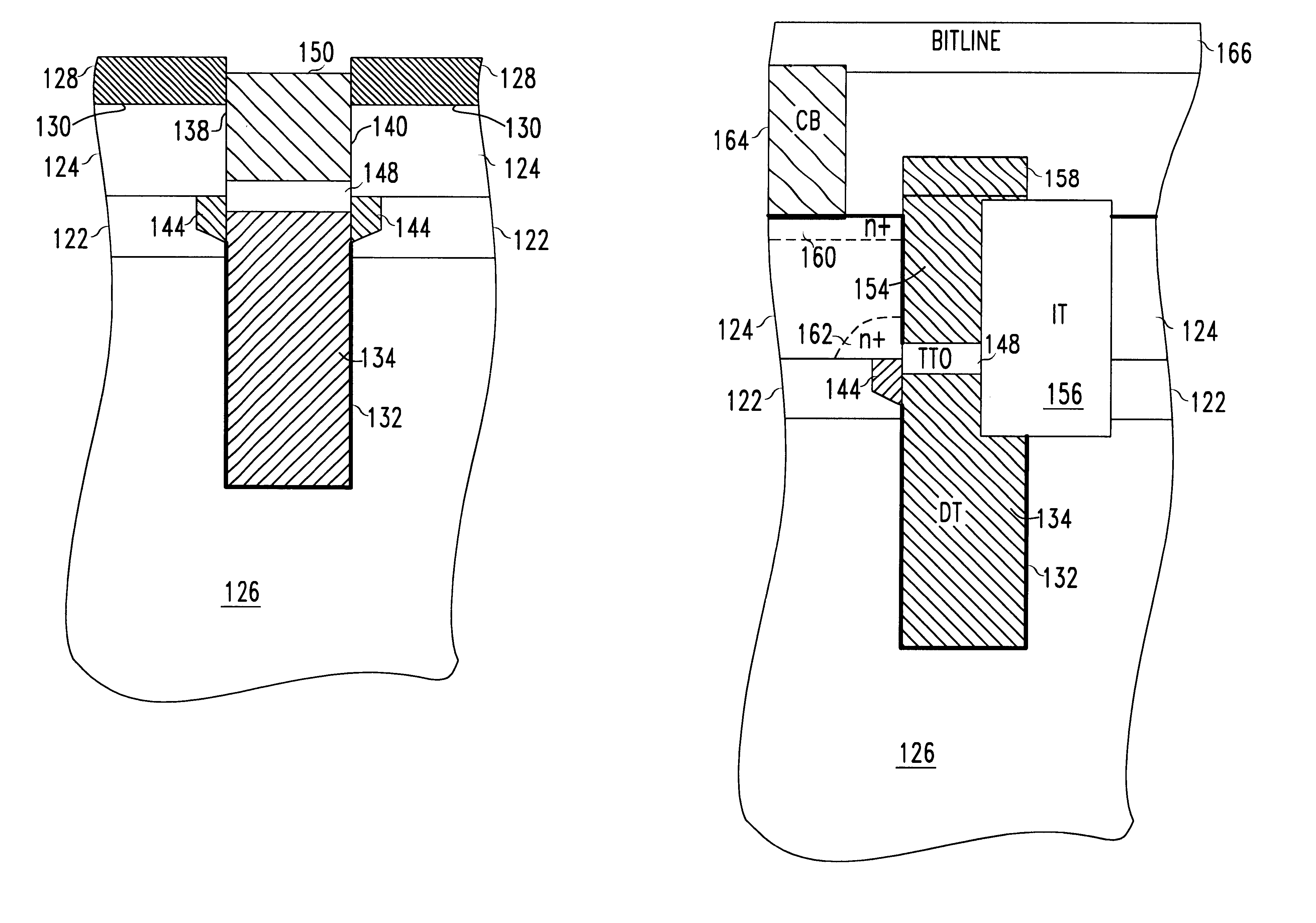
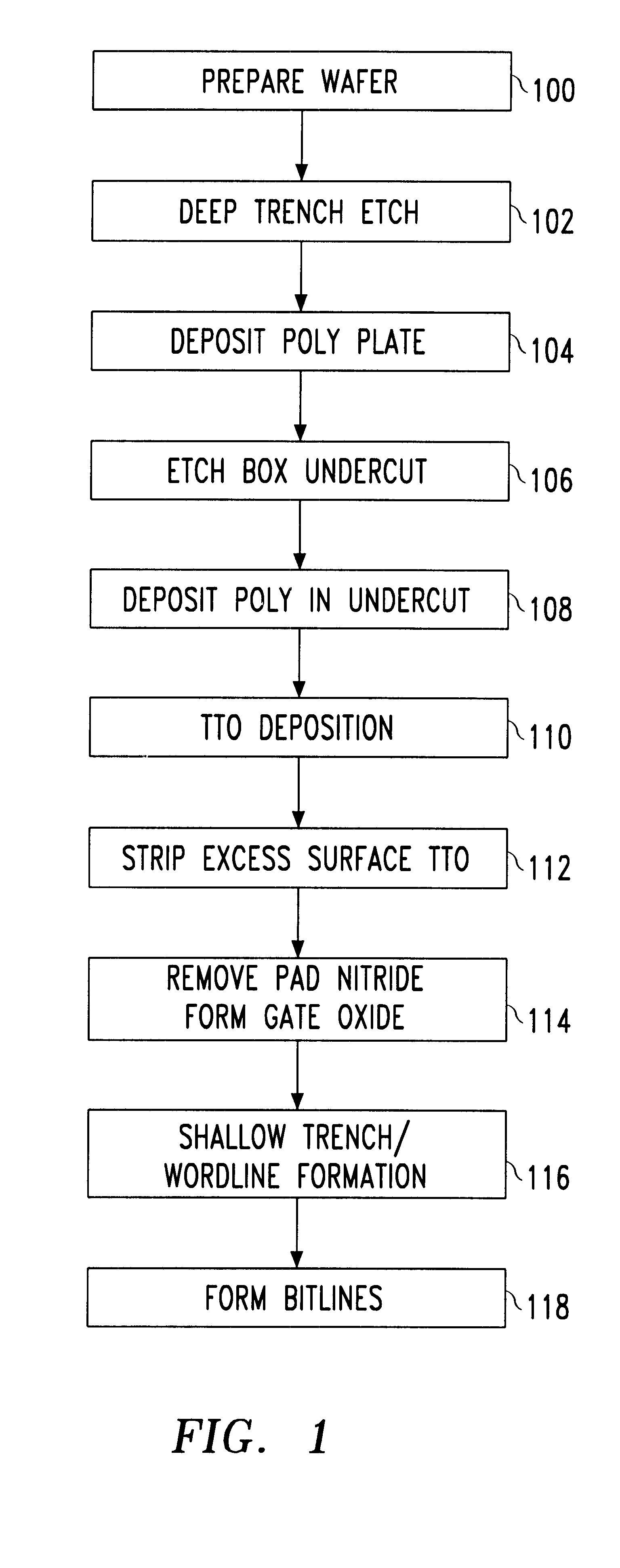
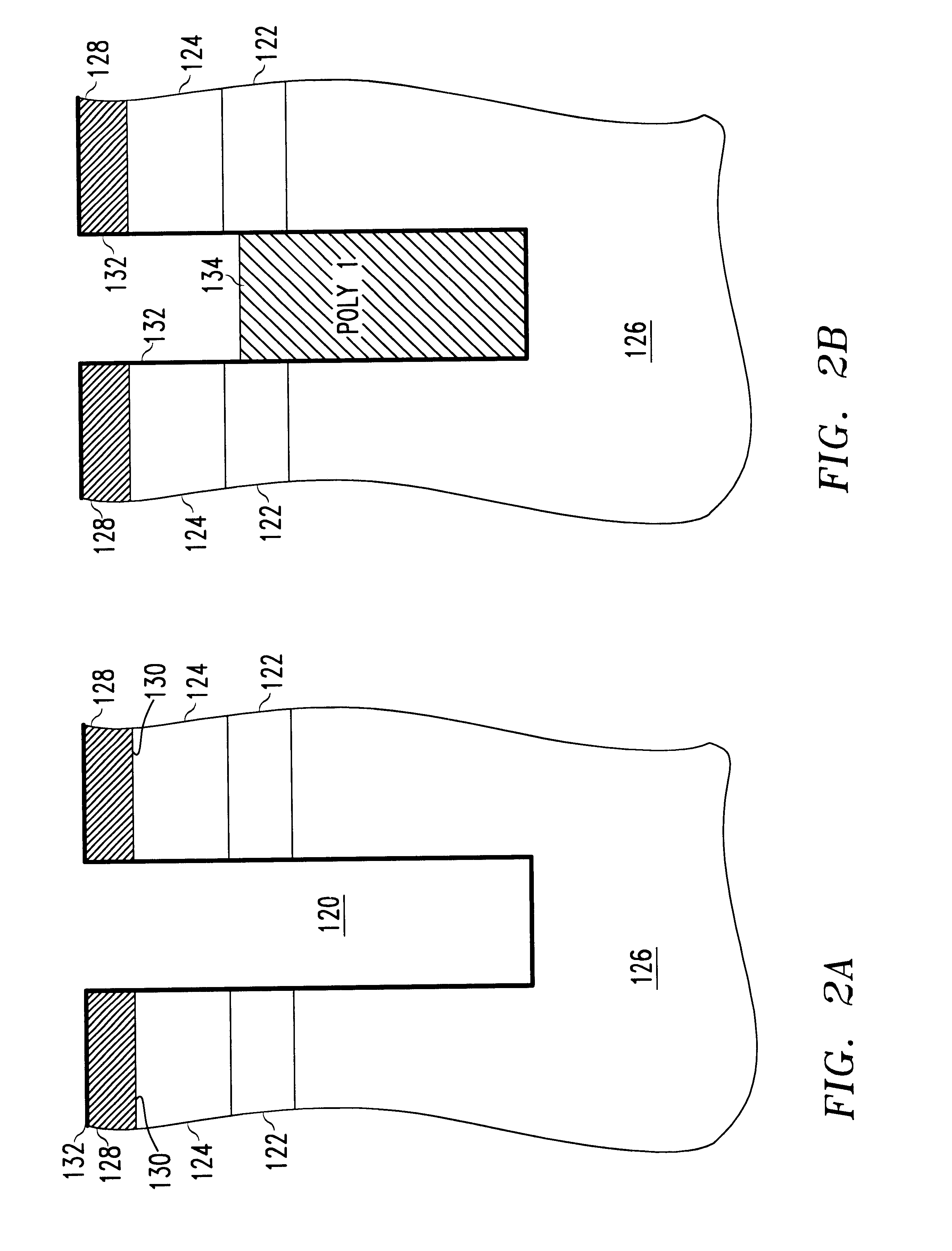
Referring now to the drawings, and more particularly, FIG. 1 shows a flow diagram of the preferred embodiment silicon-on-insulator (SOI) process for forming vertical DRAM cells. First, in step 100, a layered semiconductor wafer is prepared. Preferably, the initial wafer is a single crystal silicon wafer. A buried oxide (BOX) layer is formed in the silicon wafer. The BOX layer isolates a silicon layer (SOI layer) above the BOX layer from a thick substrate, which is much thicker than the silicon layer. Then, in step 102 deep trenches are formed, preferably, using a typical photolithographic and etch process. The deep trenches are formed through the silicon layer, the BOX layer and into the thicker substrate. A thin node dielectric layer is conformally formed on the wafer and along the deep trench sidewalls. After forming the thin node dielectric layer a capacitor plate is formed in step 104 in the deep trenches. Then, in step 106, the thin node dielectric layer is stripped from the SO...


PUM


Abstract

A silicon on insulator (SOI) dynamic random access memory (DRAM) cell, array and method of manufacture. The memory cell includes a vertical access transistor above a trench storage capacitor in a layered wafer. A buried oxide (BOX) layer formed in a silicon wafer isolates an SOI layer from a silicon substrate. Deep trenches are etched through the upper surface SOI layer, the BOX layer and into the substrate. Each trench capacitor is formed in the substrate and, the access transistor is formed on a sidewall of the SOI layer. Recesses are formed in the BOX layer at the SOI layer. A polysilicon strap recessed in the BOX layer connects each polysilicon storage capacitor plate to a self-aligned contact at the source of the access transistor. Dopant is implanted into the wafer to define device regions. Access transistor gates are formed along the SOI layer sidewalls. Shallow trenches are formed and filled with insulating material to isolate cells from adjacent cells. Wordlines and bitlines are formed to complete the memory array.

Description

1. Field of the InventionThe present invention generally relates to semiconductor memories and, more particularly, to a trench capacitor dynamic random access memory cell with a vertical silicon on insulator access transistor for semiconductor memories.2. Background DescriptionDynamic Random Access Memory (DRAM) cells are well known. A DRAM cell is essentially a capacitor for storing charge and a pass transistor (also called a pass gate or access transistor) for transferring charge to and from the capacitor. Data (1 bit) stored in the cell is determined by the absence or presence of charge on the storage capacitor. Because cell size determines chip density, size and cost, reducing cell area is one of the DRAM designer's primary goals. Reducing cell area is done, normally, by reducing feature size to shrink the cell.Besides shrinking the cell features, the most effective way to reduce cell area is to reduce the largest feature in the cell, typically, the area of the storage capacitor...

Claims


Application Information

Patent Timeline
IPC IPC(8): H01L21/70H01L21/8242H01L27/12
CPCH01L27/10864H01L27/10867H01L27/1203H10B12/0383H10B12/0385
Inventor RADENS, CARL J.BRONNER, GARY B.CHEN, TZE-CHIANGDAVARI, BIJANMANDELMAN, JACK A.MOY, DANSADANA, DEVENDRA K.SHAHIDI, GHAVAM GHAVAMISTIFFLER, SCOTT R.
Owner IBM CORP
Why Eureka
Try Eureka