Wafer probe interface arrangement with nonresilient probe elements and support structure

a non-resilient, probe element technology, applied in electrical testing, instruments, measurement devices, etc., can solve the problems of large upper and lower dies of such probe equipment, failure of the probing process, and challenge of cobra probes

Inactive Publication Date: 2002-07-30
IBM CORP
View PDF18 Cites 38 Cited by
  • Summary
  • Abstract
  • Description
  • Claims
  • Application Information

AI Technical Summary

Problems solved by technology

However, more recently on the basis of ever increasing industry demands and advances in the technology, cobra probes have been challenged in their ranges of applicability.
Thus, upper and lower dies of such probe equipment become quite large and are prone to warping or arching, which frequently leads to a failure of the probing process.
Furthermore, cobra probes employed in an extremely dense packing situation, particularly with large chips, are frequently prone to electrical shorts.
Moreover, the normally considerable length of a cobra probe renders it unsuitable for large bandwidths.
In contrast, the relatively short probes of peripherally bumped membranes could present a solution to the problem, but cannot be fully implemented because of failures related to contact resistance or non-optimized contact pressure in the implementing systems.

Method used


Image

  • Wafer probe interface arrangement with nonresilient probe elements and support structure
  • Wafer probe interface arrangement with nonresilient probe elements and support structure
  • Wafer probe interface arrangement with nonresilient probe elements and support structure

Examples


Embodiment Construction

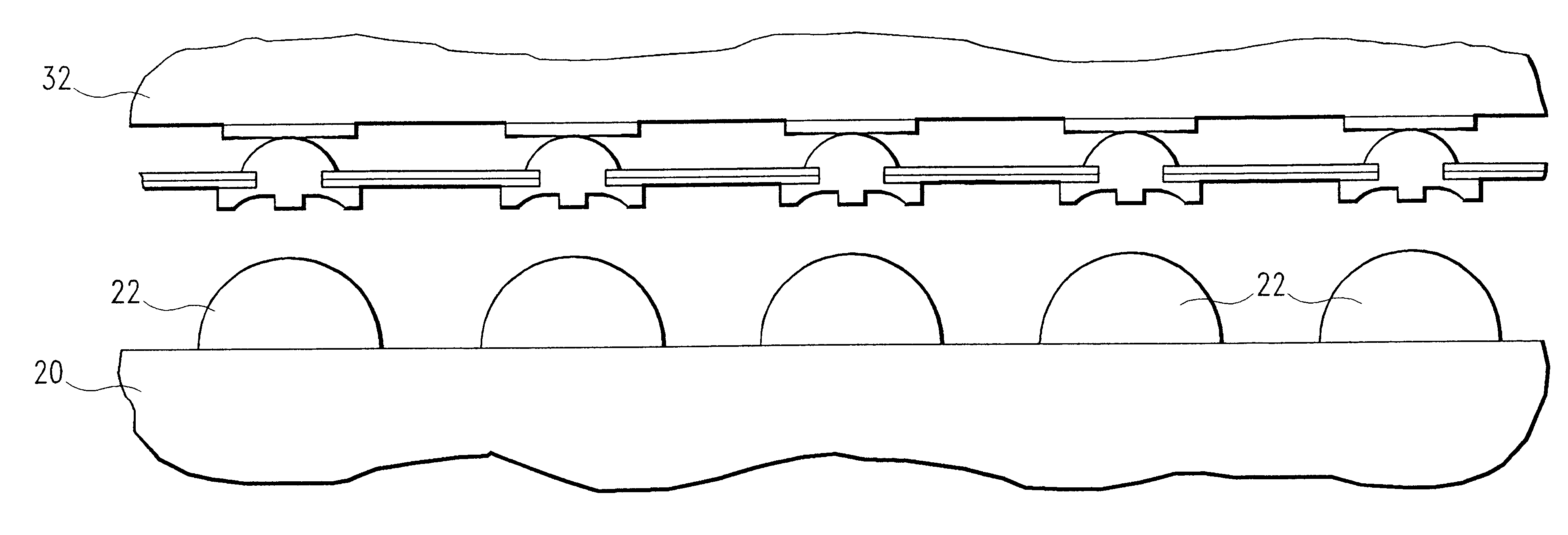
The present invention provides reliable electrical contacts between rigid probes of a variable density built on a polyimide film and devices in an undiced wafer.

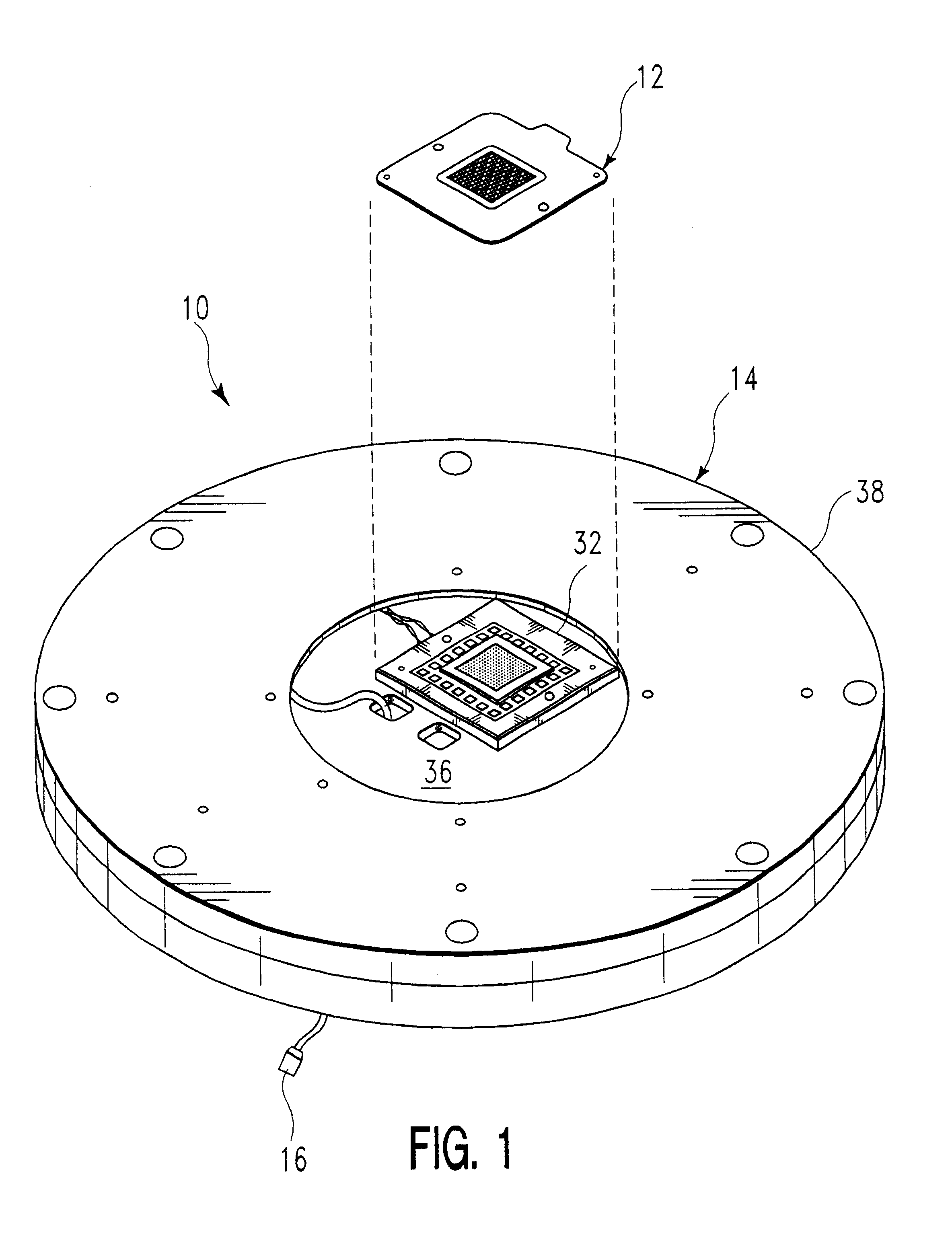
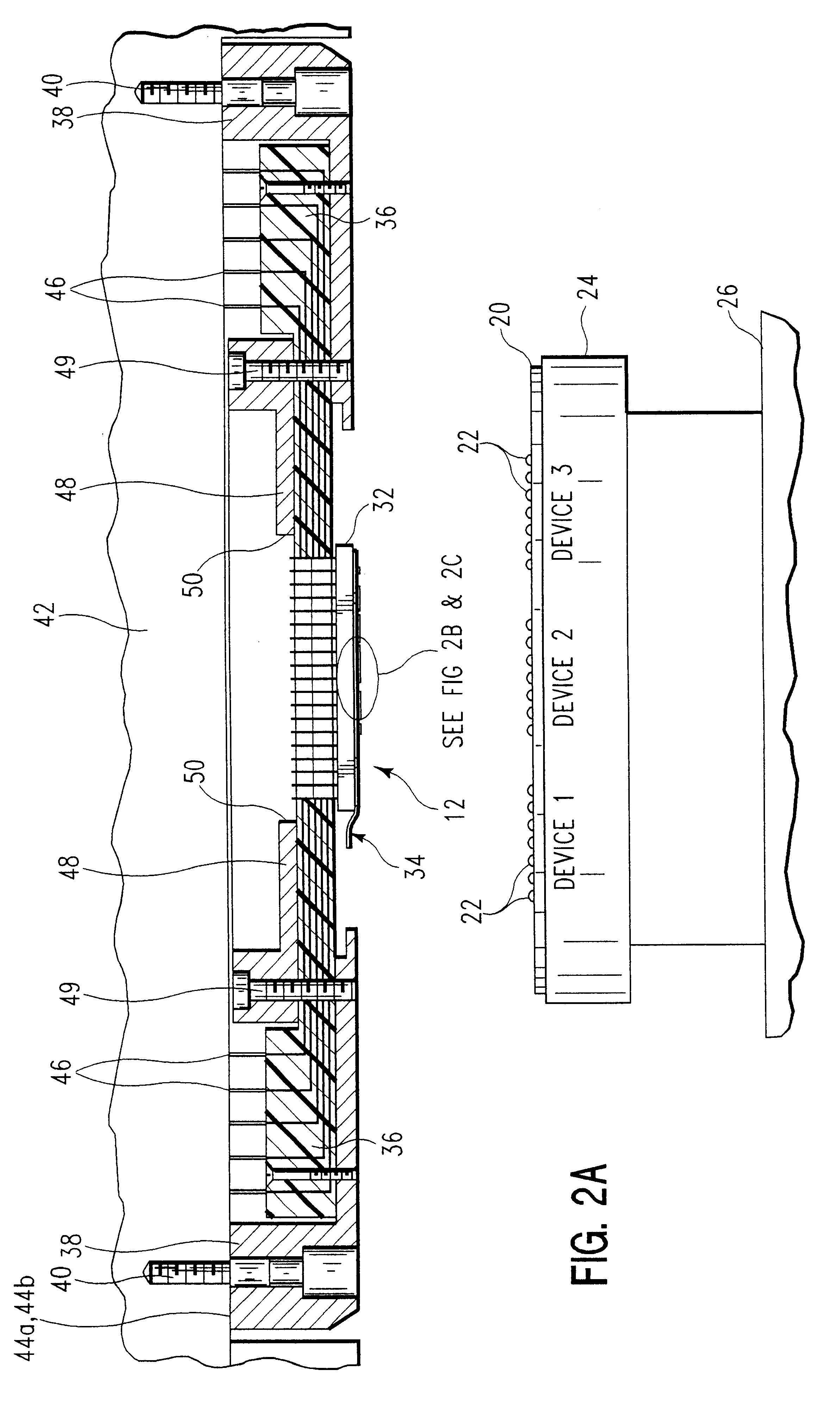
FIG. 1 illustrates a perspective view of a semiconductor wafer test system interface assembly 10 constructed pursuant to the present invention, shown inverted for purposes of clarity. FIG. 3 illustrates, in an inverted representation as in FIG. 1, an exploded perspective view of the components of the test assembly.

The test system interface assembly 10, as illustrated in FIG. 1, is designed to provide for reliable and repeatable electrical contacts. The assembly 10 comprises a typical rigid probe 12 and a space transformer 14. The rigid probe 12 is aligned into its appropriate position opposite conductive areas of a ceramic substrate 32, and is then maintained in proper contact through the use of a vacuum connection arrangement 16, 34. The test assembly nonresilient probe may be a type as disclosed in Byrnes et al., U.S. Pat....


PUM


Abstract

A nonresilient rigid test probe arrangement which is designed for testing the integrity of silicon semiconductor device wafers or chips, and which eliminates pliant conditions encountered by current text fixtures, which are adverse to the attainment of satisfactory test results with rigid probes. The test system interface assembly includes a rigid ceramic substrate which forms a pedestal over which the rigid probe makes electrical contact. A PC board is located on the opposite side of the ceramic substrate. A clamp ring retains the PC board to a test head system with mating precision reference surfaces formed therebetween. Pogo pin connectors extend between the PC board and the test head system. A stiffening element having a control aperture is bolted through the PC board to the clamp ring, all of which form a rigid test probe arrangement.

Description

The present invention relates to a nonresilient test probe which is designed to uniformly contact pads of semiconductor devices, and more particularly pertains to a nonresilient or rigid test probe arrangement which is designed for investigating the integrity of silicon semiconductor device wafers or chips.An extremely important facet of the semiconductor industry resides in being able to provide satisfactorily functioning semiconductor devices. In particular, such semiconductor devices may comprise wafers which are divided into areas which form chips, the shapes and dimensions of which are identical or as close to each other as is possible to obtain, so as to impart consistently uniform electrical properties thereto.Generally, semiconductor devices on chips are ordinarily connected to each other with thin strips of metal, referred to in the art as interconnection metallurgy, which in turn contact the wafer surface through a series of pads or bumps, each 60-100 micrometers in size a...

Claims


Application Information

Patent Timeline
Patent Type & Authority Patents(United States)
IPC IPC(8): G01R1/073
CPCG01R1/0735
Inventor DAS, GOBINDADUDA, STEVEN J.GASCHKE, PAUL M.GIAIMO, ANGELO M.TABER, JR., FREDERICK L.VETRERO, JOHN F.
Owner IBM CORP
Why Eureka
Try Eureka