Thin-film solar cells on the basis of IB-IIIA-VIA compound semiconductors and method for manufacturing same

a technology compound semiconductors, which is applied in the field of thin film solar cells on the basis of, can solve the problems of affecting the method in a detrimental way, affecting the development of flexible cis-solar cells so long, and peeling of the layers on glass substrates

Inactive Publication Date: 2002-08-06
ODERSUN
View PDF11 Cites 75 Cited by
  • Summary
  • Abstract
  • Description
  • Claims
  • Application Information

AI Technical Summary

Benefits of technology

With respect to the good adherence of the absorber layer cost-effective, very thin, mechanically rigid metal films may be used as substrate. On these substrates flexible solar cells can be produced by continuous roll-to-roll processes. In a first step the IB- and IIIA-metals are deposited in a continuous roll-to-roll process. In a second continuous roll-to-roll process the carrier film covered by the precursor is chalcogenised in a narrow-slit reactor. The process is performed such that the IB-IIIA metallic precursor is only incompletely converted into the ternary polycrystalline p-type absorber layer such that intermetallic phases of the IB- and IIIA-metals are directly located on the carrier film which metals serve as back electrode of the solar cell structure. Because of the short reaction time during the chalcogenising process and the low heat capacity of the carrier film ternary polycrystalline absorber layers may thus be deposited on thin carrier films in a continuous roll-to-roll process in an effective manner. The polycrystalline absorber layer is closely intergrown with the back electrode such that neither peeling nor flaking will occur on the flexible metal films. The deposition of a buffer layer and of a transparent front electrode in a continuous roll-to-roll process completes the process for producing these flexible thin-film solar cells.

Problems solved by technology

The low adherence of the polycrystalline absorber layers on molybdenum however leads to peeling of the layers on glass substrates and flaking on flexible tapes and hindered the development of flexible CIS-solar cells so long to a great extent.
It is disadvantageous with respect to all these arrangements that an additional component is to be introduced and that, therefore, an additional technological step for the deposition of these layers is necessary.
Moreover, this method is affected in a detrimental way by the reduced mechanical stability of copper such that relatively thick copper tapes are to be used.
Since according to this method the copper tape simultaneously forms the copper source for the absorbing layer, very pure copper tapes are to be used such that the costs of the solar cell are unnecessarily increased.

Method used


Image

  • Thin-film solar cells on the basis of IB-IIIA-VIA compound semiconductors and method for manufacturing same

Examples


Embodiment Construction

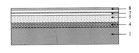
A stainless steel film typically having a thickness of 10 .mu.m to 30 .mu.m normally serves as carrier film 1. The stainless steel film may further be covered by other metals or oxides. On the carrier film 1 there is located the back electrode 4 having a thickness of 1 .mu.m to 5 .mu.m. The back electrode 4 preferably consists of the intermetallic phase Cu.sub.7 In.sub.3. The polycrystalline absorber layer (PAS) 5 of the p-type conductivity--preferably consisting of the phase CuInS.sub.2 -- is arranged thereabove. The absorber layer typically has a thickness of 1 .mu.m to 3 .mu.m. The PAS 5 is closely intergrown with the back electrode 4 such that there will not occur any flaking. A thin buffer layer 7, preferably made of CdS, is arranged on the polycrystalline absorber layer 5. This buffer layer 7 has a thickness of 10 nm to 50 nm. A transparent bleeder electrode 8, preferably made of externally doped zinc oxide, is arranged on the buffer layer 7.

This solar cell has a thickness of ...


PUM


Abstract

The invention relates to a thin-film solar cell on the basis of IB-IIIA-VIA compound semiconductors and a method for producing such a solar cell. Between the polycrystalline IB-IIIA-VIA absorber layer of the p-type conductivity and the carrier film serving as a substrate, a back electrode of intermetallic phases of the same IB- and IIIA-metals are located which are deposited for the generation of the absorber layer. The absorber layer and the back electrode are produced in such a way that the precursor consisting of IB-IIIA-metals is vertically only incompletely converted into the photovoltaicly active absorber material from the side opposite to the carrier film by reaction with chalcogen such that intermetallic phases of the IB- and IIIA-metals are directly located on the carrier film, which metals serve as back electrode of the solar cell structure.

Description

The invention relates to a thin-film solar cell on the basis of the IB-IIIA-VIA semiconductors, the back electrode of which consists of intermetallic phases of the same metals which are used for manufacturing the polycrystalline absorbing layer of the p-type conductivity. The invention further relates to a method for manufacturing such a solar cell.It is one of the main aims of the development of photovoltaic modules to substantially reduce the production costs of solar electricity for terrestrial applications. For extraterrestrial applications the reduction in weight of the solar modules is together with the radiation resistance of the solar cells in the focus of the development.Solar cells and modules on the basis of polycrystalline IB-IIIA-VIA compound semiconductors are suitable candidates in order to reach these aims. In recent years great progress could be reached particularly with compound semiconductors on the basis of copper, indium and gallium as well as selenium or sulfur...

Claims


Application Information

Patent Timeline
Patent Type & Authority Patents(United States)
IPC IPC(8): H01L31/0272H01L31/04H01L31/0264H01L31/072H01L31/06H01L31/0336H01L31/032H01L31/18H01L31/0224H01L31/0392H01L31/0749
CPCH01L31/022425H01L31/0322H01L31/03928H01L31/0749Y02E10/541Y02P70/50
Inventor TOBER, OLAFPENNDORF, JURGENWINKLER, MICHAELJACOBS, KLAUSKOSCHACK, THOMAS
Owner ODERSUN
Why Eureka
Try Eureka