Capacitive circuit array for fingerprint sensing

a circuit array and fingerprint sensing technology, applied in the field of two-dimensional mapping of fingerprint patterns, can solve the problems of complex and expensive, high cost, and high cost of prior art optical scanning methods, and achieve the effect of low cost and economical manufacturing

Inactive Publication Date: 2002-08-06
SENTRONICS CORP
View PDF5 Cites 25 Cited by
  • Summary
  • Abstract
  • Description
  • Claims
  • Application Information

AI Technical Summary

Benefits of technology

The present invention utilizes sensor electrodes, having three or more metal electrodes/lines per pixel at the topmost layer of the sensor; at least two input voltage lines of different phases and one or more of sensor pickup electrodes. This combination nulls out the DC background capacitance and thus no electronic circuitry below the sensor electrodes is required. The sensor array can be manufactured without the need for expensive and slow vacuu...

Problems solved by technology

In the area of the fingerprint sensor, the primary prior art systems utilize an optical scanning method which is relatively bulky and expensive due to the optics, lasers and the CCD array utilized.
The first two categories are complex and expensive to make, and thus most of recent development activiti...

Method used


Image

  • Capacitive circuit array for fingerprint sensing
  • Capacitive circuit array for fingerprint sensing
  • Capacitive circuit array for fingerprint sensing

Examples


Embodiment Construction

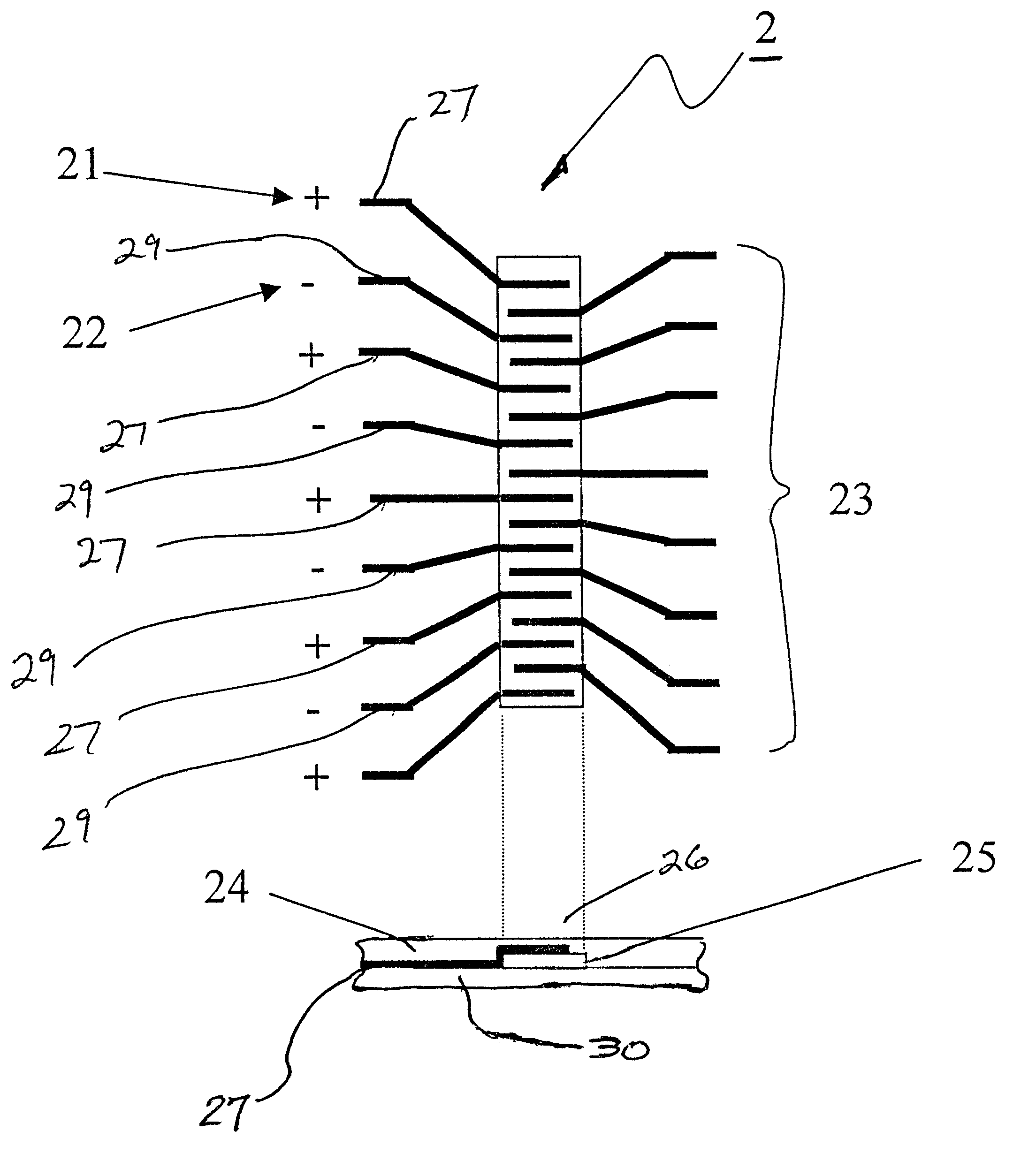
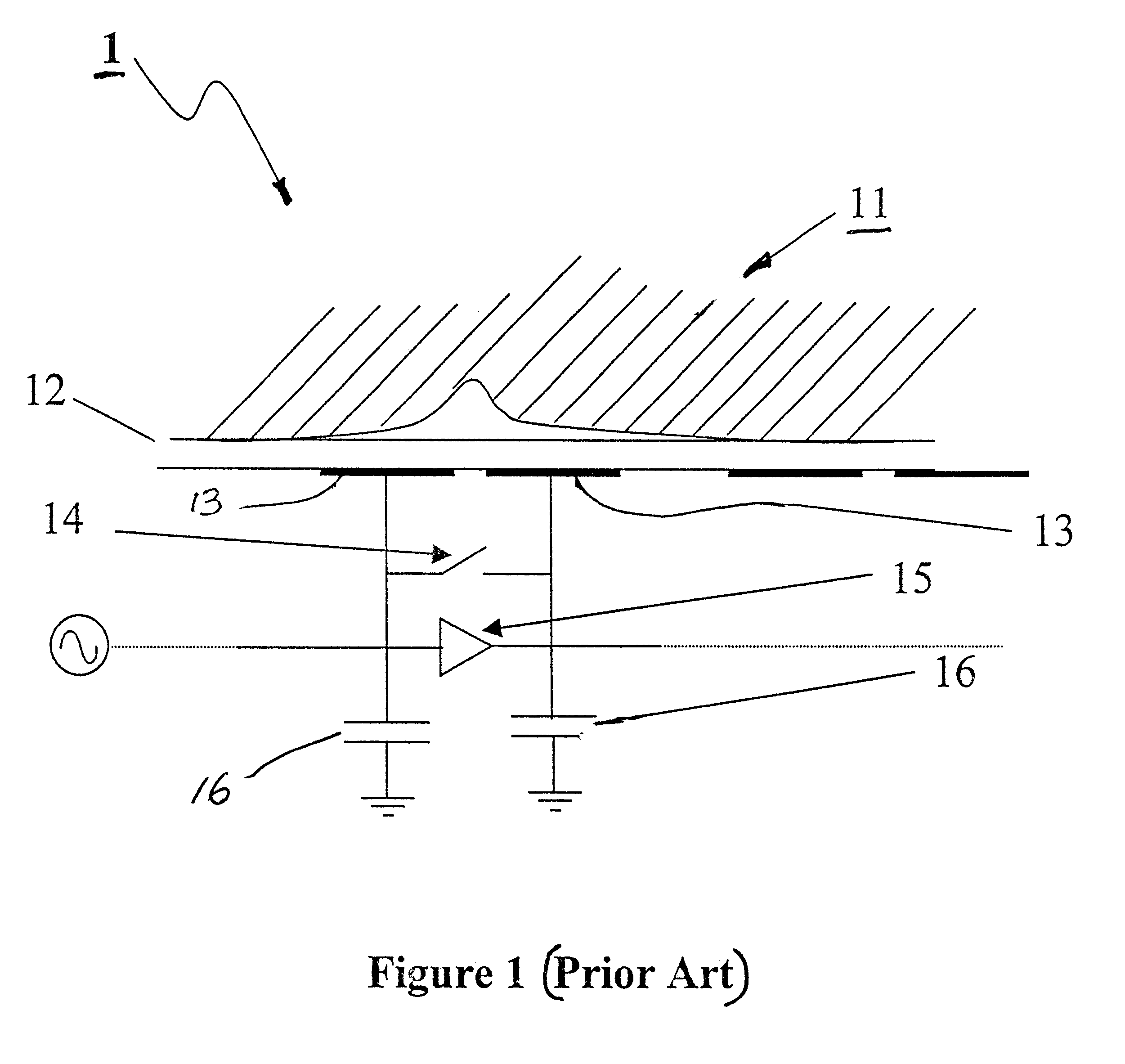
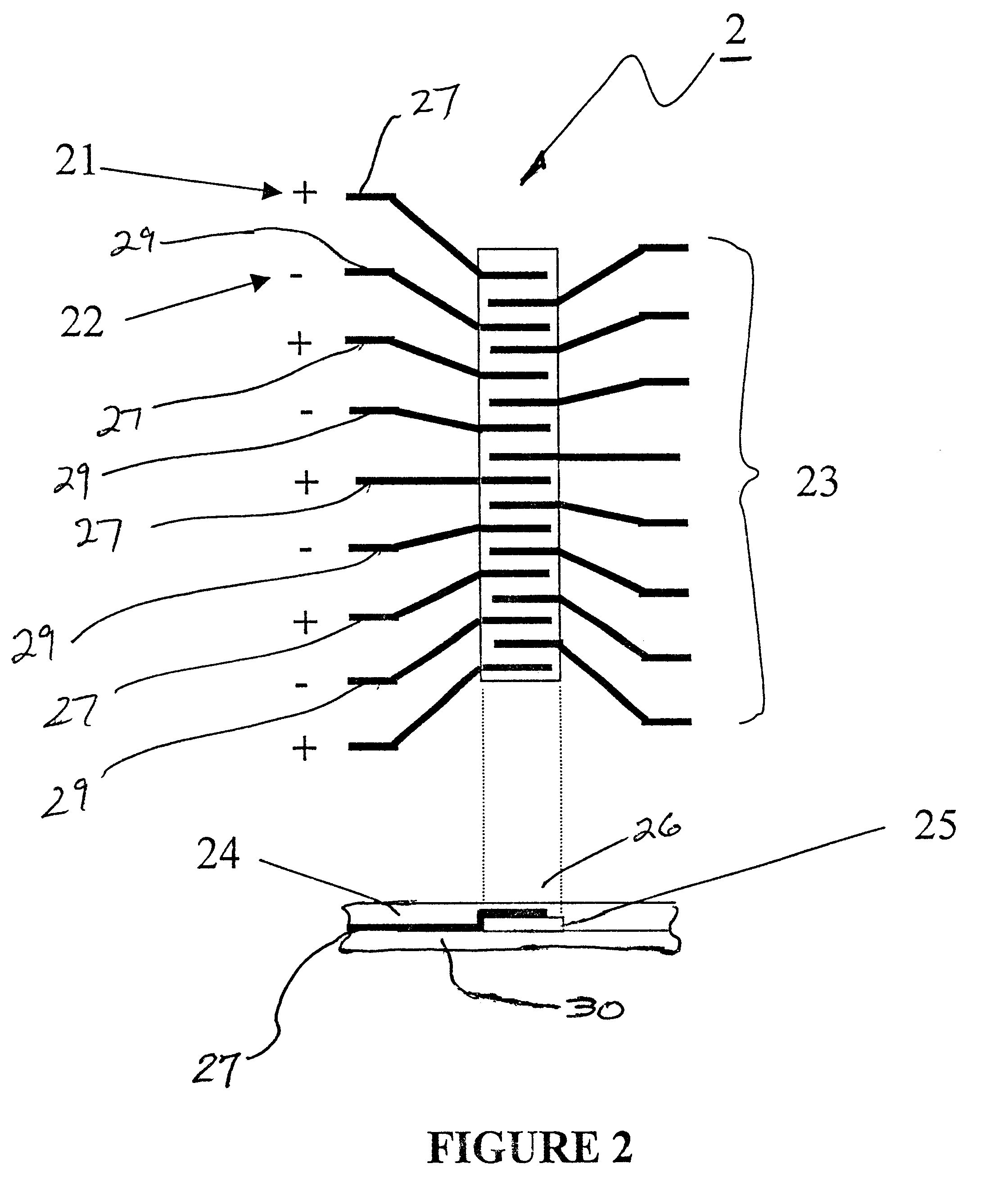
FIG. 1 illustrates a prior art fingerprint sensing device 1. The circuitry for each pixel (only one illustrated) comprises amplifier 15, switch 14 and two capacitors 16 (a pixel is defined as an elementary set of patterns which repeats in the array and consists of pick up voltage electrodes which are necessary to perform sensing of finger ridge lines at a point or at a small point-like region). The capacitive readout between the two pickup electrodes, or conductive layers, 13 is passed through the circuit to remove the large background and parasitic capacitance. A thin protective coating 12 is disposed between the pickup electrodes 13 and the finger 11. The circuitry requires fabrication of many transistors per pixel with sub-micron resolution processing which in turn requires expensive and slow semiconductor process equipment. In addition, the silicon wafer and other processing material costs are also high with a limited wafer size per process, yielding relatively small numbers of ...


PUM


Abstract

A compact sensor which maps fingerprints for identification purposes. The sensor consists of an array of pixels with each pixel configured with one or more pickup conductive electrodes surrounded by voltage electrodes of different phases. This configuration performs capacitive differencing to eliminate the large background capacitance without the need for complex sensor circuitry. In addition, the readout lines are electrically shielded from the input voltage lines by an intermediate grounded conductive layer, thereby eliminating the parasitic capacitance and allowing the detection of minute capacitance variation of the finger surface.

Description

1. Field of the InventionThe present invention relates to two dimensional mapping of fingerprint patterns for identification purposes utilizing a capacitive circuit array.2. Description of the Prior ArtFingerprint sensing and the associated identification systems which include data bases and a match algorithm processor have been available in the prior art. In the area of the fingerprint sensor, the primary prior art systems utilize an optical scanning method which is relatively bulky and expensive due to the optics, lasers and the CCD array utilized. Due to this reason, there have been attempts to develop electronic means of sensing fingerprint patterns. All electronic fingerprint sensors can be categorized as follows; tactile pressure sensors, thermal sensors and capacitive sensors. The first two categories are complex and expensive to make, and thus most of recent development activities are in the area of capacitive sensors.One group of capacitive sensors rely on thin deformable m...

Claims


Application Information

Patent Timeline
IPC IPC(8): G01R27/26
CPCG01R27/2605
Inventor UM, GREGORY S.
Owner SENTRONICS CORP
Why Eureka
Try Eureka