

Manufacturing method of plasma display panel that includes adielectric glass layer having small particle sizes
a plasma display panel and adielectric glass technology, applied in the manufacture of electric discharge tubes/lamps, cold cathode manufacturing, electromechanical systems, etc., can solve the problems of limited screen size and viewing angle, glass paste does not flow well, liquid crystal display is not suitable for a large screen,
- Summary
- Abstract
- Description
- Claims
- Application Information
AI Technical Summary
Problems solved by technology
Method used
Image

Examples
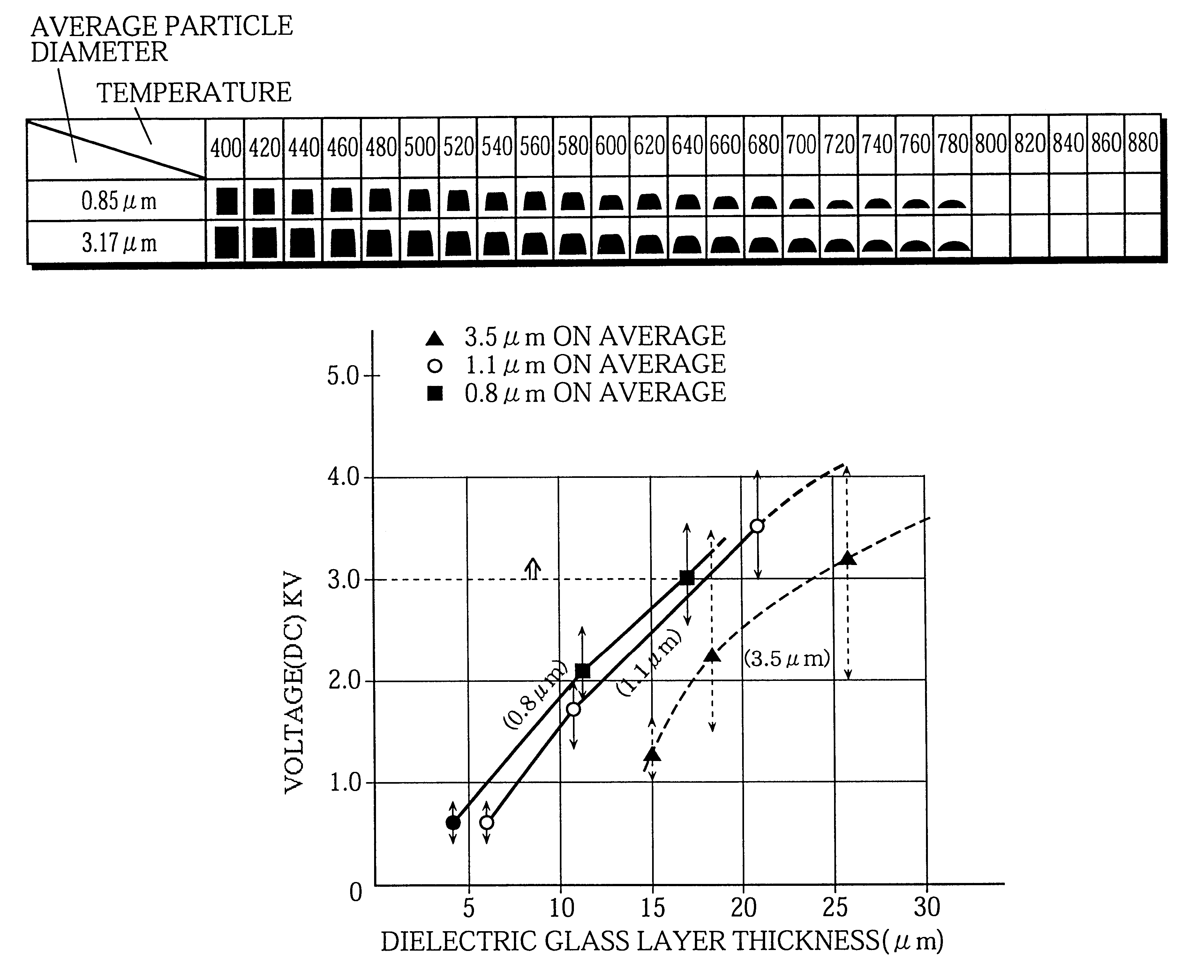
experiment 4
In the experiment 4, the voltage endurance of dielectric glass layers are measured. The dielectric glass layers have different thickness equal to or smaller than 30 .mu.m and have been formed using the glass materials in which the average particle diameters of the glass powders are 3.5 .mu.m, 1.1 .mu.m, and 0.8 .mu.m. The relation between the thickness of dielectric glass layer and the voltage endurance is shown in FIG. 12 according to the experimental results.
Study
The experimental results on Tables 5 and 6 show that the PDPs corresponding to the test samples Nos. 1 to 6, and 9 to 12 have superior panel intensities compared with a conventional PDP, the panel intensity of which is about 400 cd / m.sup.2 (described in "Flat-Panel Display" 1997, p198).
The observation of the bubble sizes, and the results of the withstand voltage test of the dielectric glass layers and the acceleration life test of the PDPs show that the PDPs corresponding to the test samples Nos. 1 to 6, and 9 to 12 inclu...
example
(2)
(Table 7)
(Table 8)
(Table 9)
(Table 10)
(Table 11)
(Table 12)
(Table 13)
(Table 14)
(Table 15)
(Table 16)
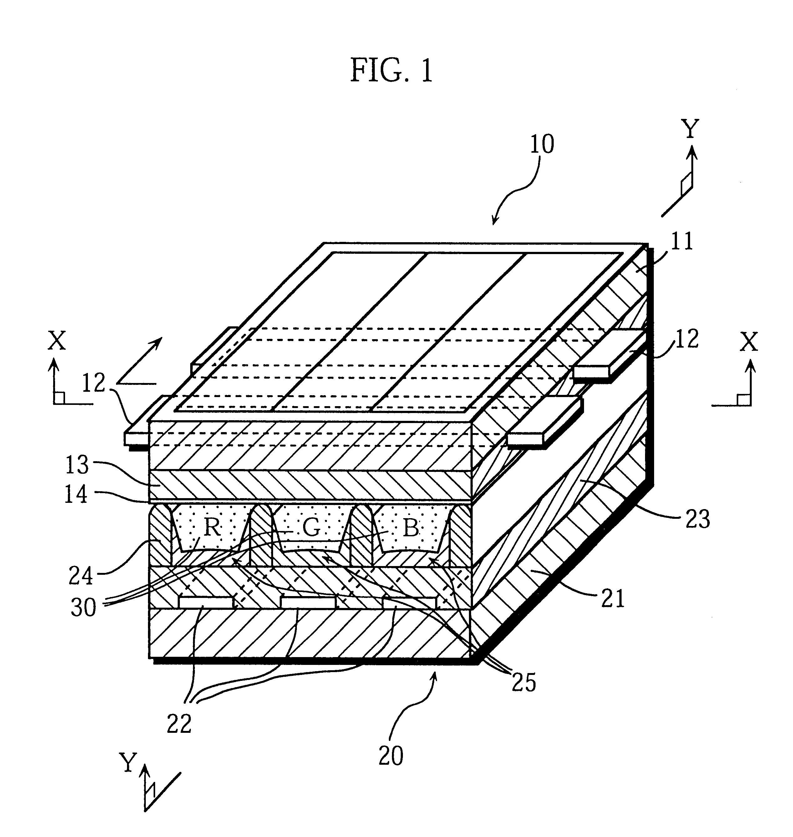
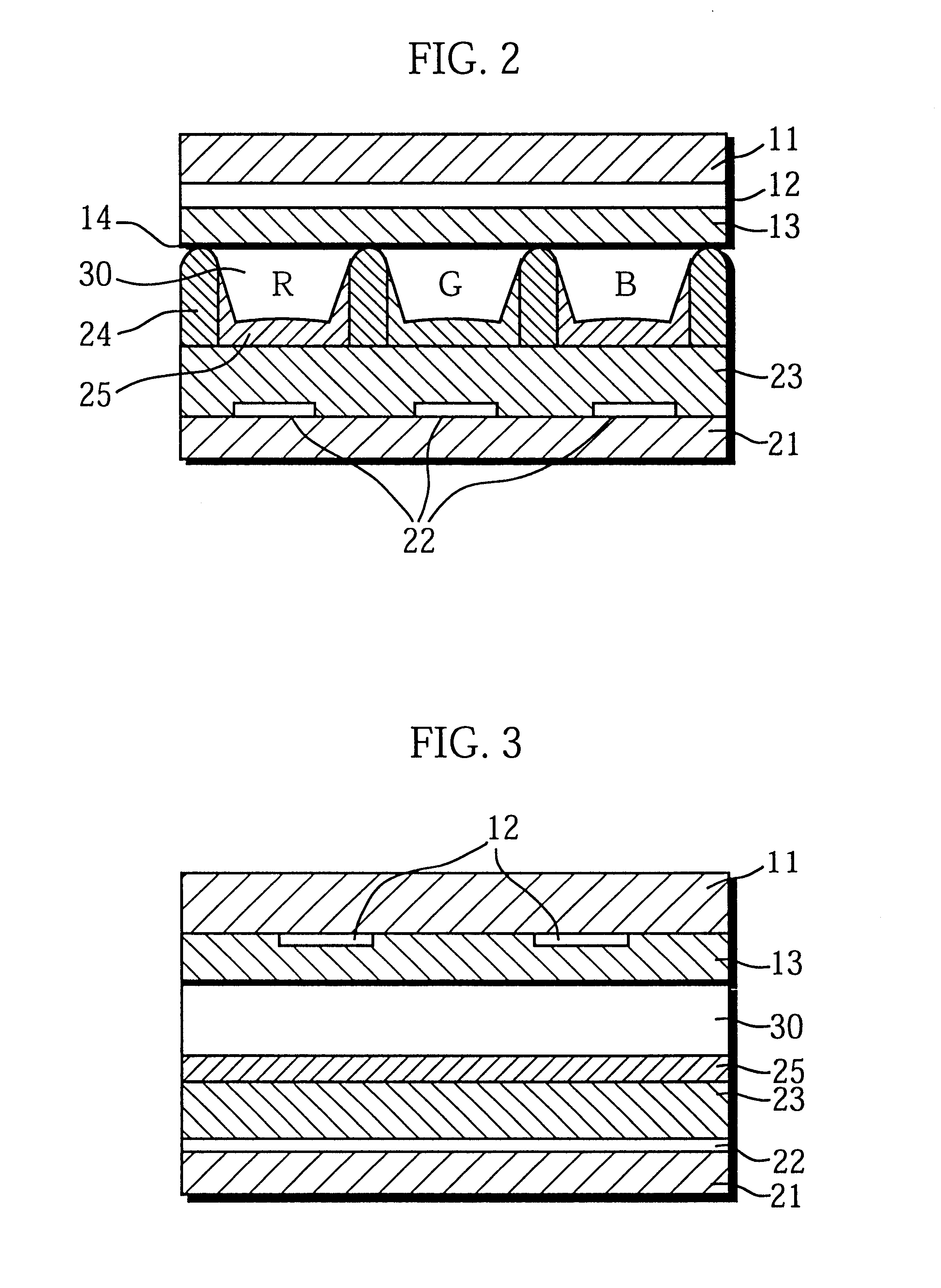
In the PDPs corresponding to the test samples Nos. 1 to 6, 9 to 12, 15 to 20, 23 to 28, and 31 to 34 on Tables 7 to 16, the discharge electrodes and the address electrodes are covered by dielectric glass layers. The dielectric glass layers are formed by applying a glass paste on the glass substrates according to the die coating method, the spray coating method, the spin coating method, or the blade coating method and by firing the applied glass paste. The glass paste includes a binder component including a plasticizer and a surface active agent, and the glass powder the average particle diameter of which is 0.1 to 1.5 .mu.m and the maximum particle diameter of which is equal to or smaller than three times the average particle diameter. The thickness of the dielectric glass layers is set to be 10 to 15 .mu.m (on average).
The cell size of the PDPs is set for the high-definition TV displ...
experiment 1
For each of the PDPs corresponding to the test samples Nos. 1 to 14, the sizes of the bubbles in the dielectric layers on the discharge electrodes and the address electrodes are examined by an electronic microscope (the magnification is 1000 times), and the average bubble diameter is obtained from the measurement of the diameters of a predetermined number of bubbles. The diameter of one bubble is the average of the measurements of two axes.
PUM
| Property | Measurement | Unit |
|---|---|---|
| particle diameter | aaaaa | aaaaa |
| particle diameter | aaaaa | aaaaa |
| wt. % | aaaaa | aaaaa |
Abstract
Description
Claims
Application Information