Semiconductor physical quantity sensor

a technology of physical quantity and semiconductor, applied in the direction of acceleration measurement using interia forces, microstructural devices, instruments, etc., can solve the problems of large sensor output error, large offset, poor temperature characteristic of sensor,

Inactive Publication Date: 2002-09-17
DENSO CORP
View PDF11 Cites 42 Cited by
  • Summary
  • Abstract
  • Description
  • Claims
  • Application Information

AI Technical Summary

Problems solved by technology

As a result, there has been the problem that the temperature characteristic of the sensor is poor.
However, in studies carried out by the present inventors into the related art semiconductor acceleration sensor described above, the problem has arisen that manufacturing process error of the sensor causes the output error of the sensor, or offset, to be large.
And when along with increases in sensor sensitivity further studies were carried out into the problem of offset, it was found that the following problems occur.
Conseq

Method used


Image

  • Semiconductor physical quantity sensor
  • Semiconductor physical quantity sensor
  • Semiconductor physical quantity sensor

Examples


first embodiment

(First Embodiment)

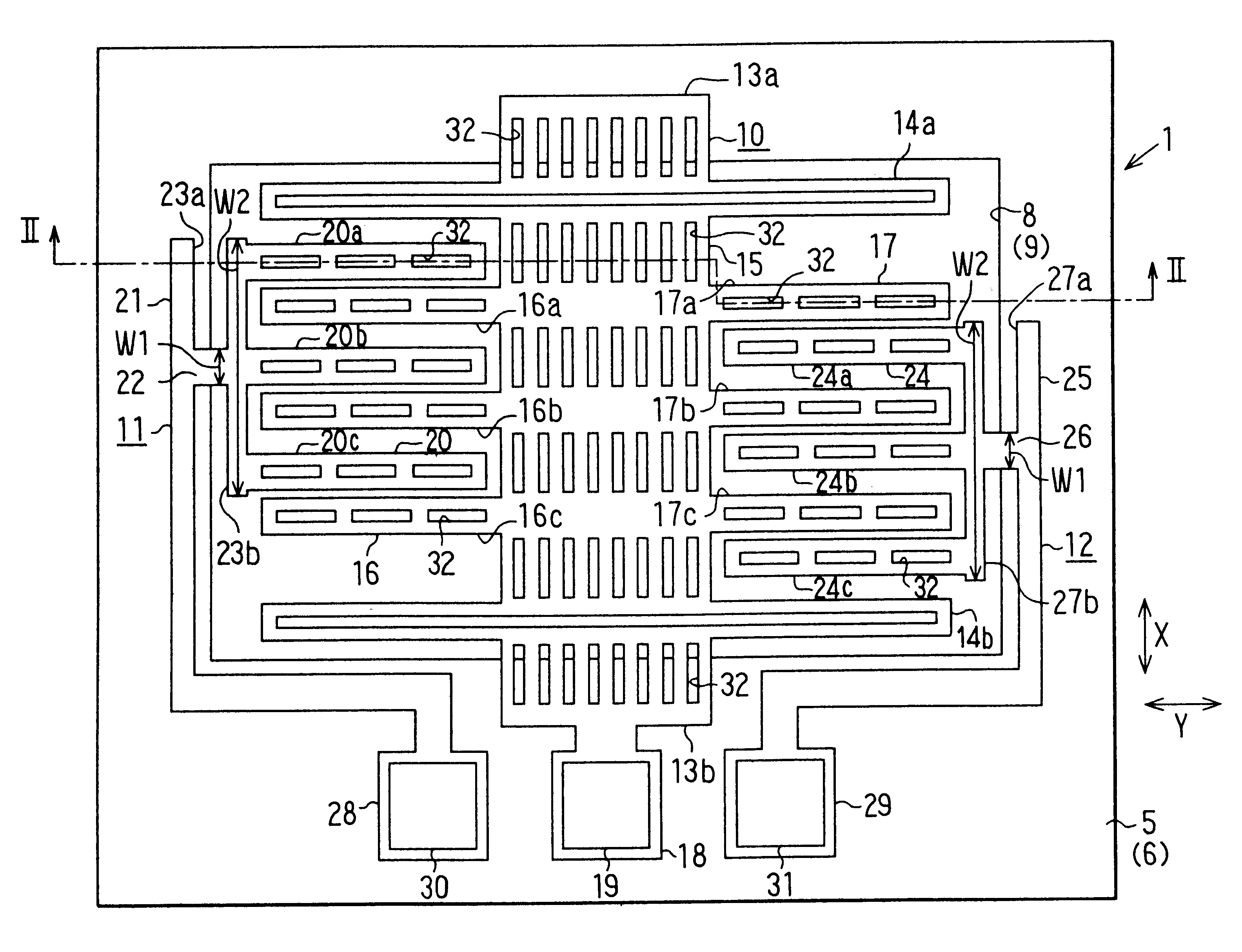
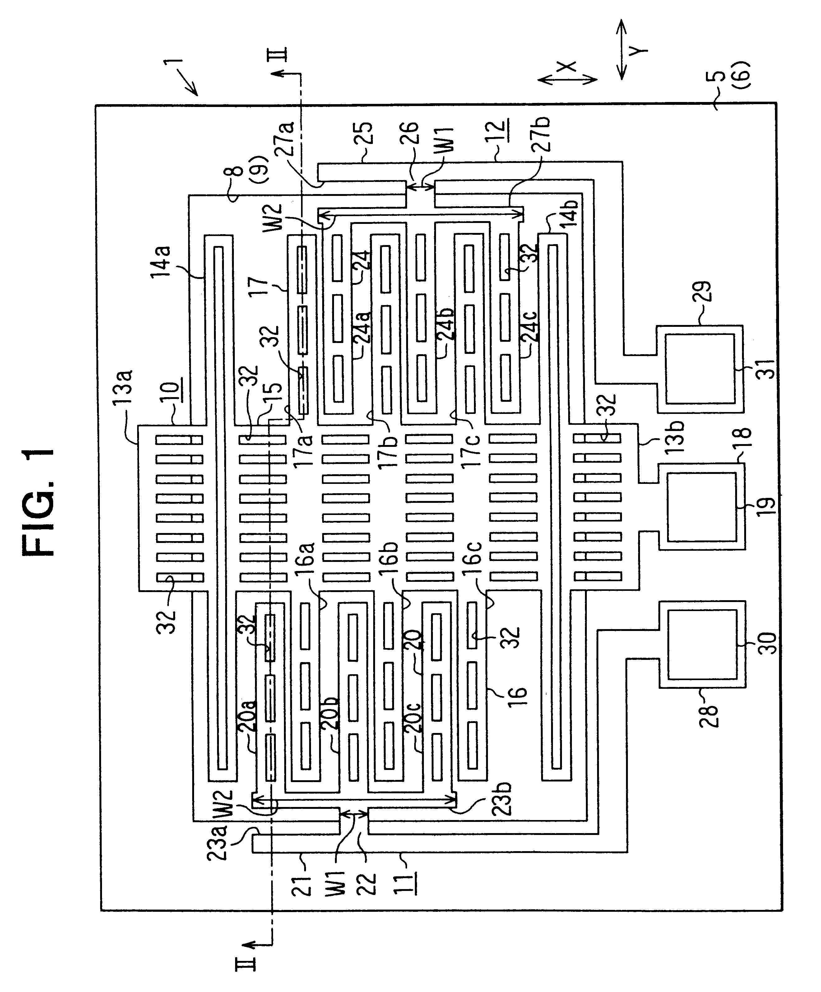
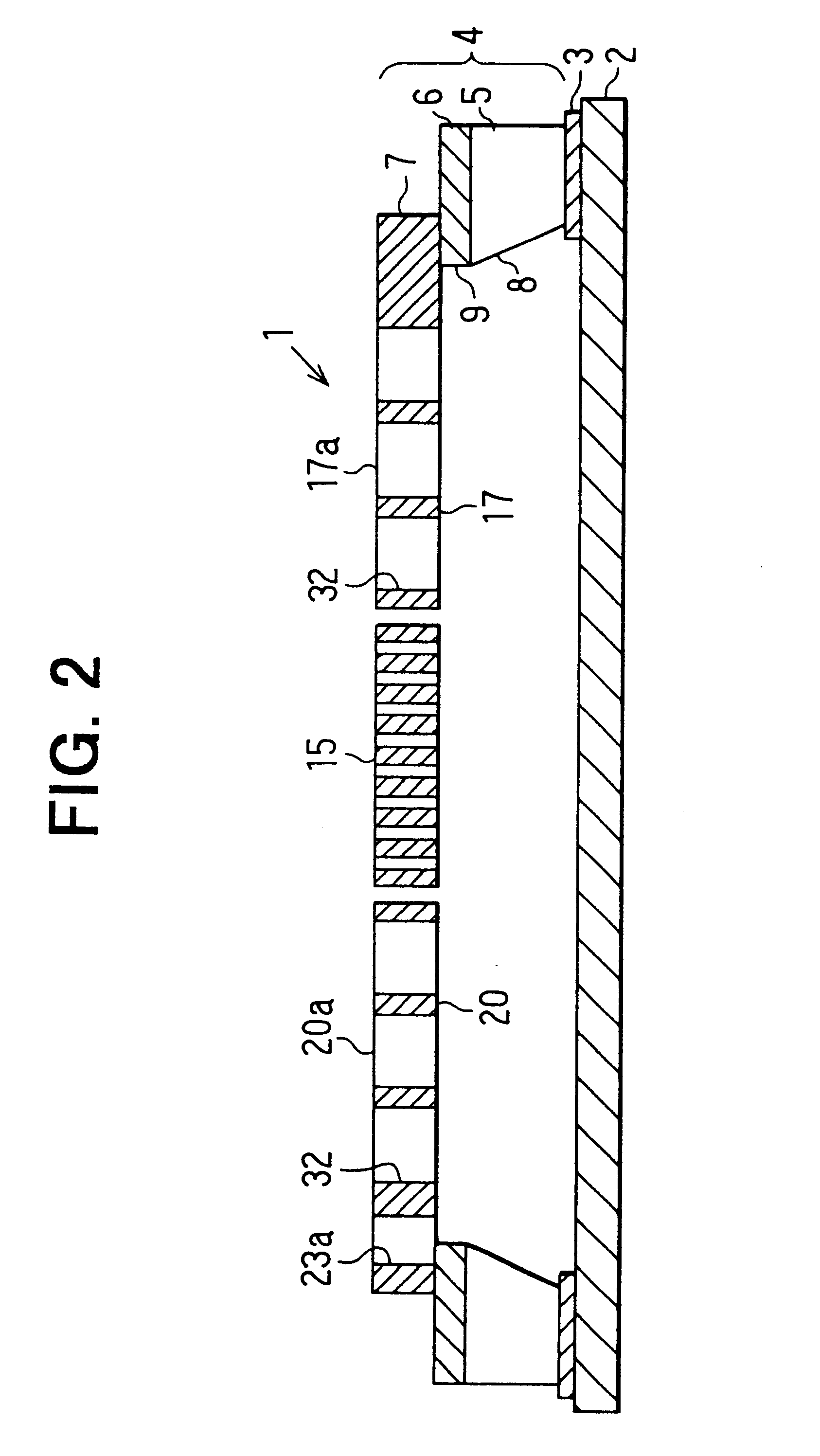
In this embodiment, the invention is applied to a differential capacitance type semiconductor acceleration sensor. A plan view of this semiconductor acceleration sensor 1 is shown in FIG. 1, and a vertical sectional view on the line II--II in FIG. 1 is shown in FIG. 2. This sensor has moving electrodes 16 (16a through 16c) and 17 (17a through 17c) provided on a bridgelike weight part 15 and cantilevered fixed electrodes 20 (20a through 20c) and 24 (24a through 24c).

As shown in FIG. 2, a sensor chip 4 is fixed on a package plate 2 by means of an adhesive 3. In this example, a SOI substrate is used as the sensor chip 4: a semiconductor thin film (monocrystalline silicon layer) 7 serving as a semiconductor substrate to be used to make sensor elements is disposed on an insulating film 6, consisting of a silicon oxide film, on a supporting substrate 5, consisting of a monocrystalline silicon substrate. The semiconductor thin film 7 is obtained by disposing a monocrystal...

second embodiment

(Second Embodiment)

In this embodiment also the invention is applied to a differential capacitance type semiconductor acceleration sensor as an example of a capacitance-detecting semiconductor physical quantity sensor, and this second embodiment has the aim of making it possible to minimize offset of the sensor by adopting a construction which is tolerant of positional deviation of an opening in one direction caused by process dispersion of the sensor. FIG. 21 is a plan view of this semiconductor acceleration sensor 100, and FIG. 22 is a schematic sectional view on the line XXII--XXII in FIG. 21.

The semiconductor acceleration sensor (hereinafter, sensor) 100, like the sensor shown in FIG. 35, is formed by carrying out known micro-machining processes on a semiconductor substrate. As shown in FIG. 22, the semiconductor substrate of the semiconductor acceleration sensor 100 is a rectangular SOI substrate 10 having an insulating film 13 as an insulating layer between a first silicon subs...

third embodiment

(Third Embodiment)

In this embodiment also the invention is applied to a differential capacitance type semiconductor acceleration sensor, but this third embodiment has the aim of making it possible to minimize offset of the sensor by adopting a construction which not only tolerates positional deviation of an opening in one direction caused by process dispersion of the sensor but also tolerates shape deviation of the opening and thickness dispersion of the insulating layer of the semiconductor substrate. FIG. 26 is a plan view of this semiconductor acceleration sensor 200 and FIG. 27 is a schematic sectional view on the line XXVII--XXVII in FIG. 26.

The semiconductor acceleration sensor (hereinafter, sensor) 200, like the sensor of the second embodiment described in the above, is made by carrying out known micro-machining processes on a SOI substrate 10. And, as in the second embodiment, comb-shaped overhang structures consisting of a moving electrode part 230 and first and second fixe...


PUM


Abstract

A semiconductor physical quantity sensor from which a stable sensor output can be obtained even when the usage environment changes. A silicon thin film is disposed on an insulating film on a supporting substrate, and a bridge structure having a weight part and moving electrodes and cantilever structures having fixed electrodes are formed as separate sections from this silicon thin film. The moving electrodes provided on the weight part and the cantilevered fixed electrodes are disposed facing each other. Slits are formed at root portions of the cantilevered fixed electrodes at the fixed ends thereof, and the width W1 of the root portions is thereby made narrower than the width W2 of the fixed electrodes proper. As a result, the transmission of warp of the supporting substrate to the cantilevered fixed electrodes is suppressed.

Description

This application is based upon Japanese Patent Application Nos. Hei. 11-210805 filed on Jul. 26, 1999, and Hei. 11-212734 filed on Jul. 27, 1999, the contents of which are incorporated herein by reference.1. Field of the InventionThis invention relates to semiconductor physical quantity sensors for detecting a physical quantity such as acceleration or angular velocity, and particularly to a capacitance-detecting type semiconductor physical quantity sensor, wherein a moving electrode part and a fixed electrode part facing this moving electrode part are formed by forming trenches in a semiconductor layer of a supporting substrate consisting of a semiconductor and an applied physical quantity is detected on the basis of variation in a capacitance between these moving and fixed electrode parts.2. Related ArtSemiconductor acceleration sensors include those of a differential capacitance type. The construction of a differential capacitance type semiconductor acceleration sensor of related ...

Claims


Application Information

Patent Timeline
IPC IPC(8): B81B3/00G01P15/08G01P15/125
CPCB81B3/0086G01P15/0802G01P15/125B81B2201/0235B81B2203/0109B81B2203/051G01P2015/0814
Inventor SAKAI, MINEKAZUMURATA, MINORUAOYAMA, SEIKINAKAGAWA, YOUKO
Owner DENSO CORP
Why Eureka
Try Eureka