Display panel filter and method of making the same

a technology of display panel and filter, applied in the field of display panel filter, can solve the problems of electromagnetic interference (emi) emissions, new problems have arisen, and the display requires a significant depth dimension

Inactive Publication Date: 2002-10-22
TRU VUE
View PDF22 Cites 50 Cited by
  • Summary
  • Abstract
  • Description
  • Claims
  • Application Information

AI Technical Summary

Problems solved by technology

First, a CRT display requires a significant depth dimension relative to the size of its display screen to accommodate a generally funnel shaped rearward portion for generation and deflection of the electron beam.
Second, most CRT screens are curved.
Although plasma display panels provide significant advantages and improvements by facilitating relatively large visual displays with a reduced panel depth and by otherwise facilitating the use of displays in environments with space restrictions which preclude the use of conventional CRT displays, new problems have arisen.
These problems relate to the quality of the visual display, increased infrared (IR) and electromagnetic interference (EMI) emissions, low contrast ratio and consumer safety issues.
This adversely affects the quality of the display.
Further, operation of the plasma display panel produces or has the potential of producing infrared (IR) emissions which are capable in some cases of interfering with a remote control of the panel or other devices utilizing infrared signaling.
Still further, operation of the plasma display panel results in the generation and emission of electromagnetic interference (EMI).
Accordingly, many plasma panel displays fail to meet governmental TCO and FCC requirements for EMI emissions and the stricter standards for various military, aircraft and other uses.
The above problems necessary limit the applicability and desirability of using plasma display panels.

Method used


Image

  • Display panel filter and method of making the same
  • Display panel filter and method of making the same
  • Display panel filter and method of making the same

Examples


Embodiment Construction

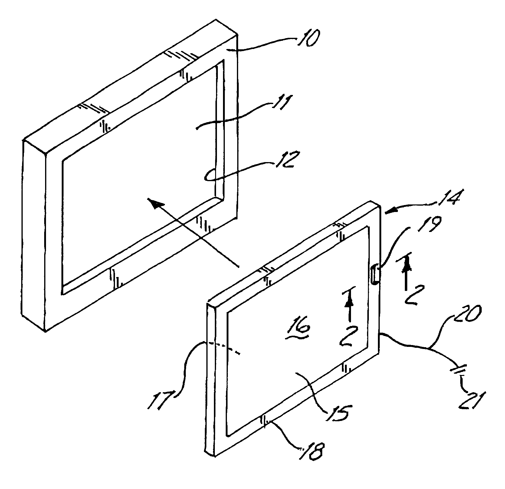
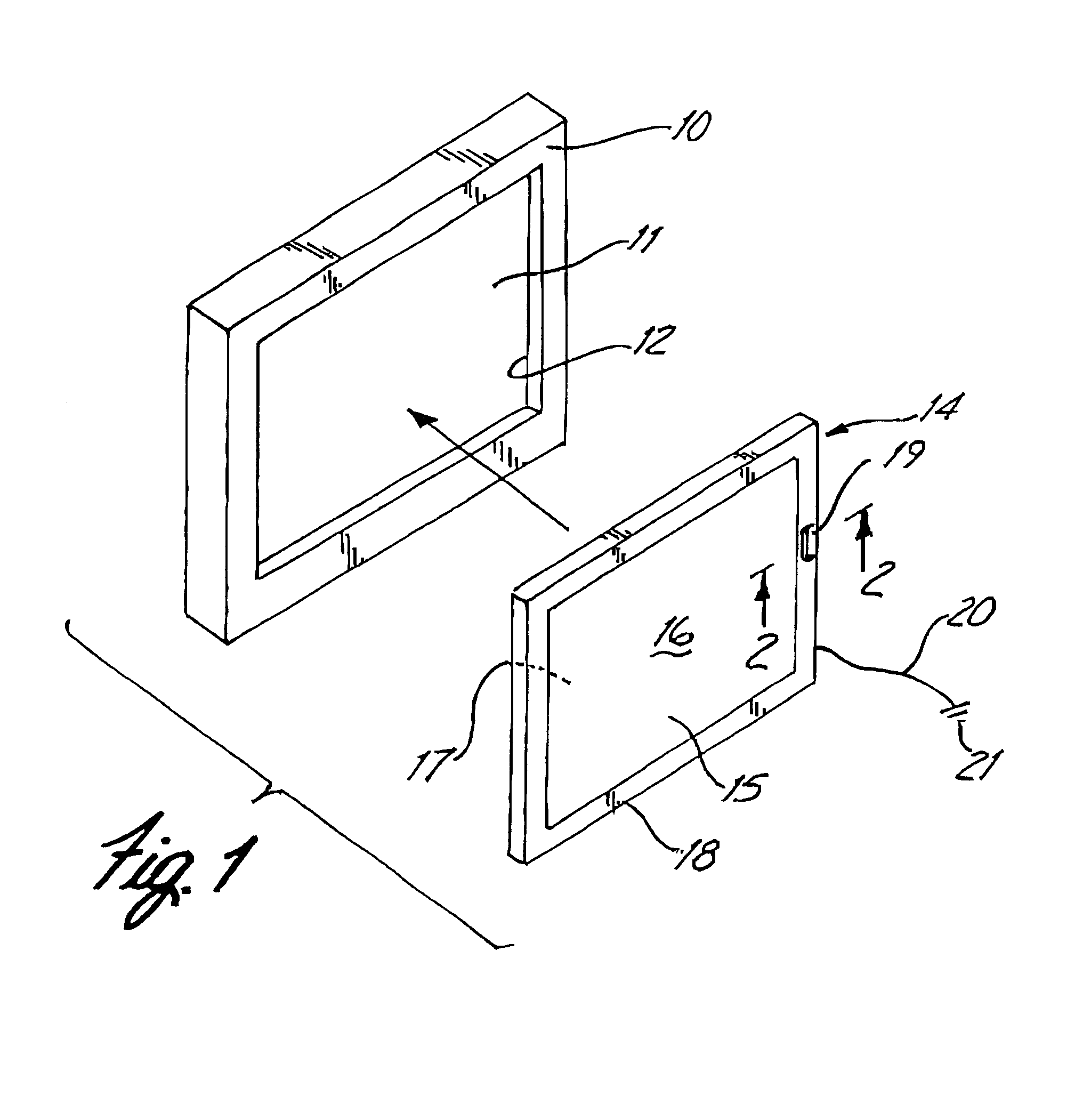
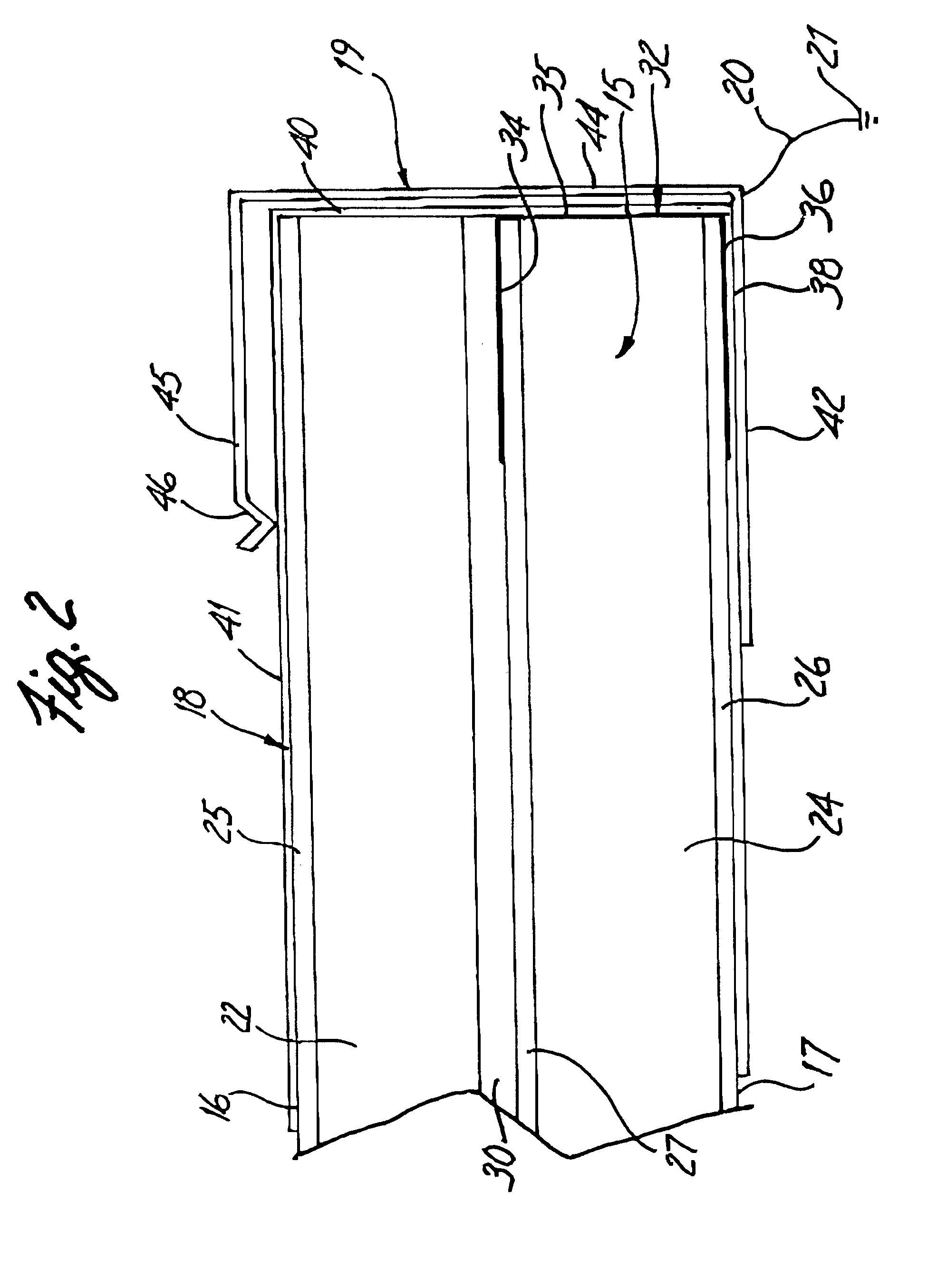
In its broadest aspect, the present invention relates to a plasma display panel filter comprised of first and second outer substrates and a filter portion positioned between the substrates and functioning to provide EMI and IR shielding capabilities and antireflective (AR) capability. This filter portion includes one or more dielectric layers sandwiched between the outer substrate. In one embodiment, the conductive layers and the non-conductive or dielectric layers are applied separately as disclosed in FIG. 5 of the present application and in pending U.S. application Ser. No. 08 / 970,771 filed Nov. 14, 1997, the entirety of which is incorporated herein by reference. In another embodiment, the conductive and dielectric layers are applied in a single film on one of the substrates prior to laminating the substrates together. This embodiment is disclosed in FIGS. 2, 3 and 4 of the present application.

Reference is first made to FIG. 1 illustrating an exploded, isometric view of a plasma ...


PUM

PropertyMeasurementUnit
refractive indexaaaaaaaaaa
optical thicknessaaaaaaaaaa

Abstract

The present invention provides a device in the form of a single filter which is useable in conjunction with a plasma display panel and which functions to reduce reflection after assembly to acceptable levels, to increase contrast enhancement ratios, to reduce EMI emissions to levels which comply with consumer safety regulations and with military and aircraft standards and to reduce infrared transmission in the 800 nm-1000 nm range to a level which does not interfere with IR remote control operation. The present invention also relates to a method of making such a plasma display panel filter.

Description

1. Field of the InventionThe present invention relates generally to a display panel filter, and more particularly to a filter having particular application for use with a plasma display panel. The present invention also relates to a method of making such a filter.2. Description of the Prior ArtVisual display panels commonly known as plasma display panels or flat panel displays have been recently introduced for the purpose of displaying visual images or information on relatively large, flat screens. Plasma display panel technology utilizes selectively energized inert gas ions to bombard phosphors on a display screen, similar to an electron beam bombarding phosphors on a cathode ray tube (CRT) screen. Plasma display panels are similar to CRT displays in that both provide a means for visually displaying information or images from an input signal; however, important differences exist. First, a CRT display requires a significant depth dimension relative to the size of its display screen ...

Claims


Application Information

Patent Timeline
Patent Type & Authority Patents(United States)
IPC IPC(8): G02B1/11G02B1/10G02B5/00H04N5/72G02B5/22G09F9/00
CPCB32B17/10174B32B17/10834G02B1/116G02B5/00H04N5/72H01J2211/446G09G3/10
Inventor WOODRUFF, DANIEL P.KUHLMANN, BRUCE E.WOLFE, JESSE D.
Owner TRU VUE
Why Eureka
Try Eureka