Spacer suitable for use in flat panel display

a flat panel display and spacer technology, applied in the manufacture of electrode systems, tubes with screens, electric discharge tubes/lamps, etc., can solve the problems of flat panel display collapse, faceplate or backplate structure of flat panel display may also fail, display breakag

Inactive Publication Date: 2002-12-03
CANON KK
View PDF77 Cites 27 Cited by
  • Summary
  • Abstract
  • Description
  • Claims
  • Application Information

AI Technical Summary

Problems solved by technology

If unopposed, this force can make the flat panel display collapse.
The faceplate or backplate structure of a flat panel display may also fail due to external forces resulting from impacts sustained by the flat panel display.
However, polyimide spacers may be inadequate because of: 1) insufficient strength; 2) inability to match the coefficient of thermal expansion of polyimide with the coefficient of thermal expansion of the materials typically used for the faceplate (e.g., glass), backplate (e.g., glass, ceramic, glass-ceramic or metal) and addressing grid (e.g., glass-ceramic or ceramic), resulting in breakage of the display; and 3) low required processing temperatures.
The low temperature tolerance prevents the use of assembly methods and materials in the display that would otherwise be available.
However, glass may not have adequate strength.
Further, micro-cracks that are inherent in glass make glass spacers even weaker than "ideal" glass because of the tendency of micro-cracks to propagate easily throughout the glass spacers.
For any spacer material, the presence of spacers may adversely affect the flow of electrons toward the faceplate structure in the vicinity of the spacers.
For example, stray electrons may electrostatically charge the surface of a spacer, changing the voltage distribution near the spacer from the desired distribution and resulting in distortion of the electron flow, thereby causing distortions in the image produced by the display.

Method used


Image

  • Spacer suitable for use in flat panel display
  • Spacer suitable for use in flat panel display
  • Spacer suitable for use in flat panel display

Examples


Embodiment Construction

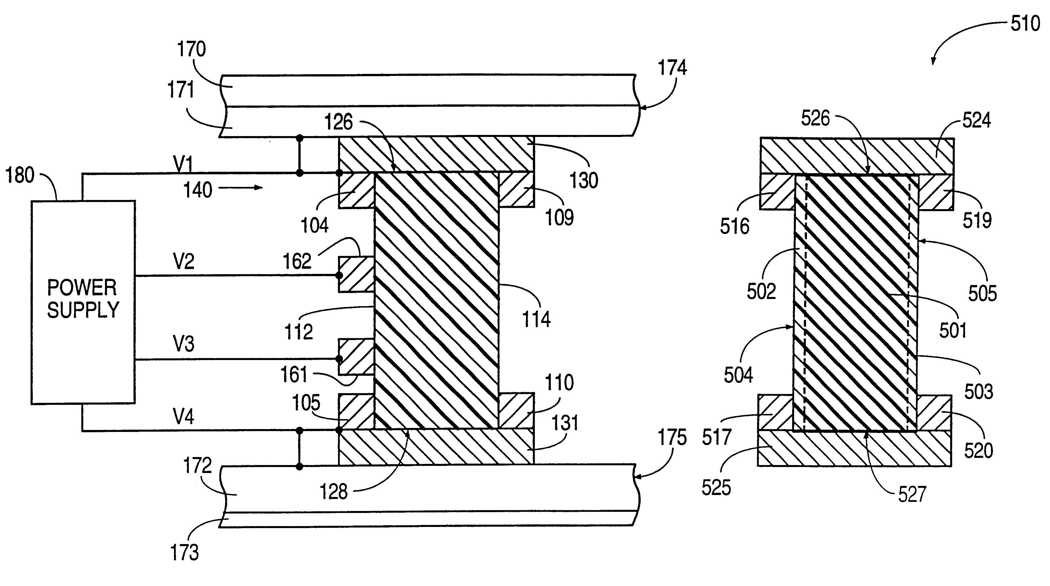
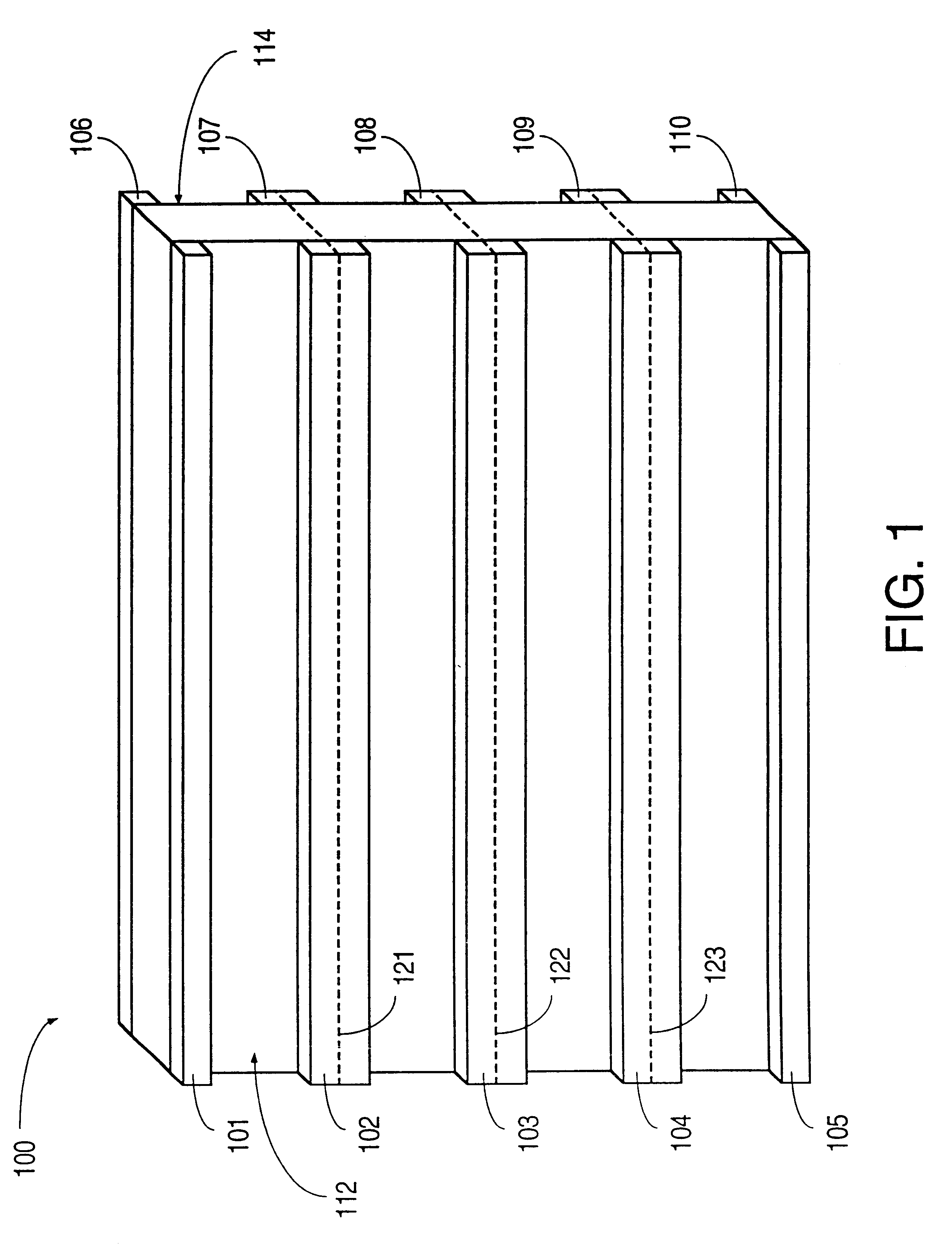
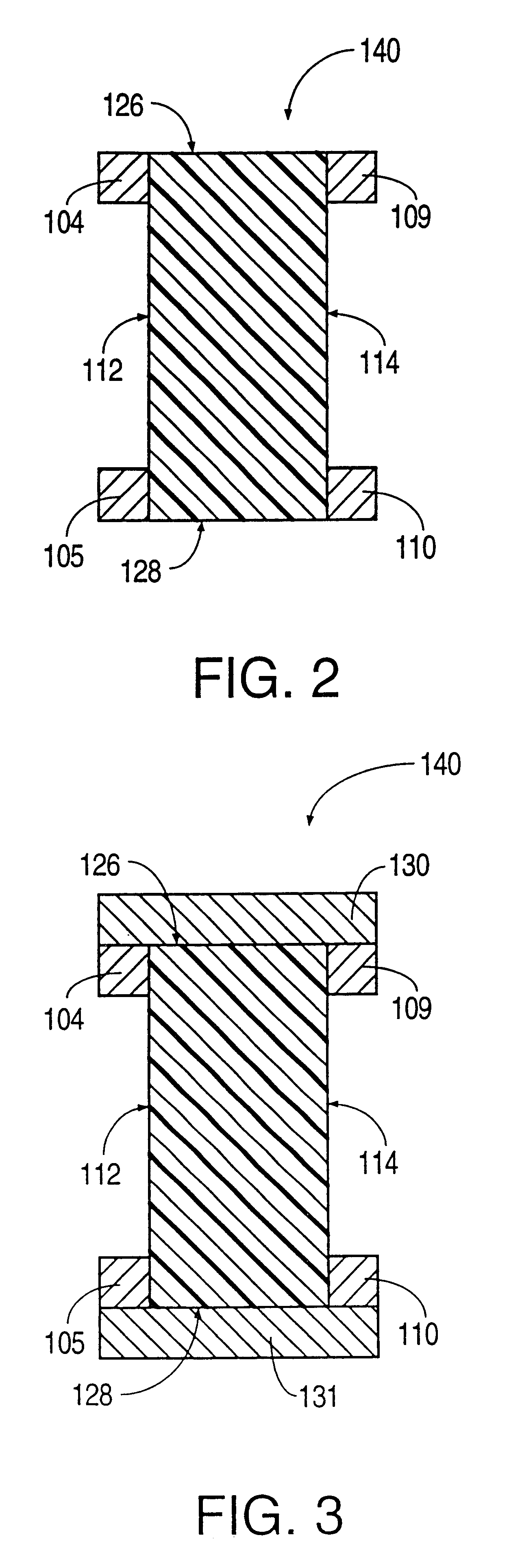
The following definitions are used in the description below. Herein, the term "electrically insulating" (or "dielectric") generally applies to materials having a resistivity greater than 10.sup.12 ohm-cm. The term "electrically non-insulating" thus refers to materials having a resistivity below 10.sup.12 ohm-cm. Electrically non-insulating materials are divided into (a) electrically conductive materials for which the resistivity is less than 1 ohm-cm and (b) electrically resistive materials for which the resistivity is in the range of 1 ohm-cm to 10.sup.12 ohm-cm. These categories are determined at low electric fields.

Examples of electrically conductive materials (or electrical conductors) are metals, metal-semiconductor compounds, and metal-semiconductor eutectics. Electrically conductive materials also include semiconductors doped (n-type or p-type) to a moderate or high level. Electrically resistive materials include intrinsic and lightly doped (n-type or p-type) semiconductors. ...


PUM

PropertyMeasurementUnit
thicknessaaaaaaaaaa
thicknessaaaaaaaaaa
dew pointaaaaaaaaaa

Abstract

A spacer (140) suitable for use in a flat panel display is formed with ceramic, transition metal, and oxygen. At least part of the oxygen is bonded to the transition metal or / and constituents of the ceramic to form a uniform electrically resistive material having a resistivity of 105-1010 ohm-cm and a secondary electron emission coefficient of less than 2 at 2 kilovolts.

Description

1. Field of the InventionThis invention relates to flat panel devices such as a flat cathode ray tube (CRT) display. More particularly, this invention relates to a spacer structure for internally supporting a faceplate structure and a backplate structure of a flat panel device.2. Related ArtNumerous attempts have been made in recent years to construct a flat CRT display (also known as a "flat panel display") to replace the conventional deflected-beam CRT display in order to provide a lighter and less bulky display. In addition to flat CRT displays, other flat panel displays, such as plasma displays, have also been developed.In flat panel displays, a faceplate structure, a backplate structure, and connecting walls around the periphery of the faceplate and backplate structures form an enclosure. In some flat panel displays, the enclosure is held at vacuum pressure, e.g., typically 1.times.10.sup.-7 torr or less. The faceplate structure includes an insulating faceplate and a light emit...

Claims


Application Information

Patent Timeline
Patent Type & Authority Patents(United States)
IPC IPC(8): H01J29/70H01J29/18H01J19/00H01J19/42C04B35/64H01J5/03H01J9/02H01J9/24H01J9/18H01J11/02H01J17/04H01J17/49H01J19/44H01J29/02H01J29/08H01J29/46H01J29/86H01J29/87H01J31/12H01J61/30
CPCH01J9/242H01J29/028H01J29/085H01J29/467H01J29/864H01J31/123H01J31/127H01J61/30H01J9/185H01J2329/8655Y10T156/1077H01J2329/8625H01J2329/863H01J2329/864H01J2329/8645Y10T156/1052Y10T156/1082Y10T156/1093
Inventor SCHMID, ANTHONY P.SPINDT, CHRISTOPHER J.MORRIS, DAVID L.FAHLEN, THEODORE S.SUN, YU NAN
Owner CANON KK
Why Eureka
Try Eureka