Dual cell reading and writing technique

a memory cell and double-cell technology, applied in the direction of digital storage, instruments, transistors, etc., can solve the problems of reducing the reading reducing the speed of the whole array reading speed, and reducing so as to increase the speed of programming and the effect of increasing the lifetime of the memory cell array

Inactive Publication Date: 2002-12-10
SANDISK TECH LLC
View PDF8 Cites 36 Cited by
  • Summary
  • Abstract
  • Description
  • Claims
  • Application Information

AI Technical Summary

Benefits of technology

Briefly and generally, the cells of a memory array are programmed in a new, pair wise programming scheme. The cells are programmed by the application of a data-independent high voltage and a data-dependent low voltage. This novel programming scheme and voltage assignment has the advantage of increasing the speed of the programming and the lifetime of the memory cell array.
According to one aspect of the invention a new programming scheme is introduced. The cells of a memory cell array are programmed in a novel, pair wise scheme. The programmed pairs of cells are separated by at least one memory cell, reducing the possibility of interference between the pairs during programming. This scheme is capable of programming all cells of the array in three programming cycles. Previous methods, which program every fourth or every seventh memory cell of an array in one cycle, are only capable of programming all cells of the array in four or seven cycles, respectively.
According to another aspect of the invention new programming voltage assignments are introduced. The memory cells of an array are typically associated with two bit lines. In existing memory systems a relatively high voltage is applied to one of the cell's bit lines, if the cell is to be programmed, while applying a low voltage to the second bit line of the cell irrespective whether the cell is to be programmed or not. The programming circuit elements, including input / output circuitry, buses, and drivers, have to be capable of handling these relatively high voltages. This is achieved, among others, by increasing the thickness of the oxide layers of the involved semiconductor devices. Devices with thicker oxide layers, however, operate slower, eventually reducing the speed of reading of the whole array.
The novel programming voltage assignments according to an aspect of the invention eliminate the necessity of thicker semiconductor layers in the programming circuit elements because the memory cell is programmed by applying the relatively high voltage to one of the bit lines irrespective whether the cell is to be programmed or not. The programming of the cell is controlled instead by the voltage applied to the second bit line of the cell. Both the programming and the non-programming voltages, applied to the second bit line, are lower than the relatively high voltage applied to the first bit line. Therefore the programming circuit elements, including the input / output circuitry, buses, and drivers, can all operate at lower voltages. This allows for utilizing thinner oxide layers, thus enhancing the operating speed of the programming circuit elements and eventually the overall performance of the circuit.
The lifetime of memory cells is also affected by the above programming scheme and programming voltage assignments. As mentioned above, every time a high voltage is applied to a bit line, some degree of wear occurs, shortening the lifetime of the cell. In the pair wise programming scheme, however, the application of the high programming voltage to one bit line programs two memory cells. Therefore high programming voltages have to be applied only half as often as in previous schemes to program all the cells of the array, increasing the lifetime of the memory system.

Problems solved by technology

Devices with thicker oxide layers, however, operate slower, eventually reducing the speed of reading of the whole array.

Method used


Image

  • Dual cell reading and writing technique
  • Dual cell reading and writing technique
  • Dual cell reading and writing technique

Examples


Embodiment Construction

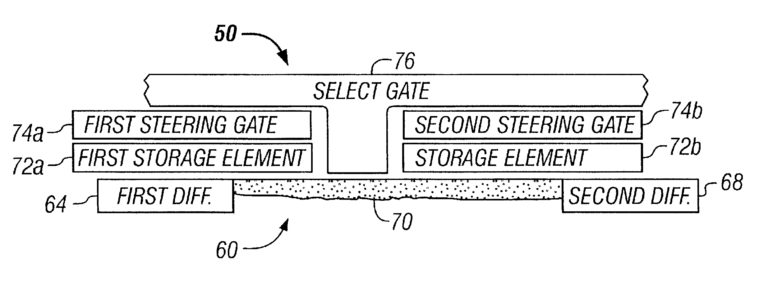
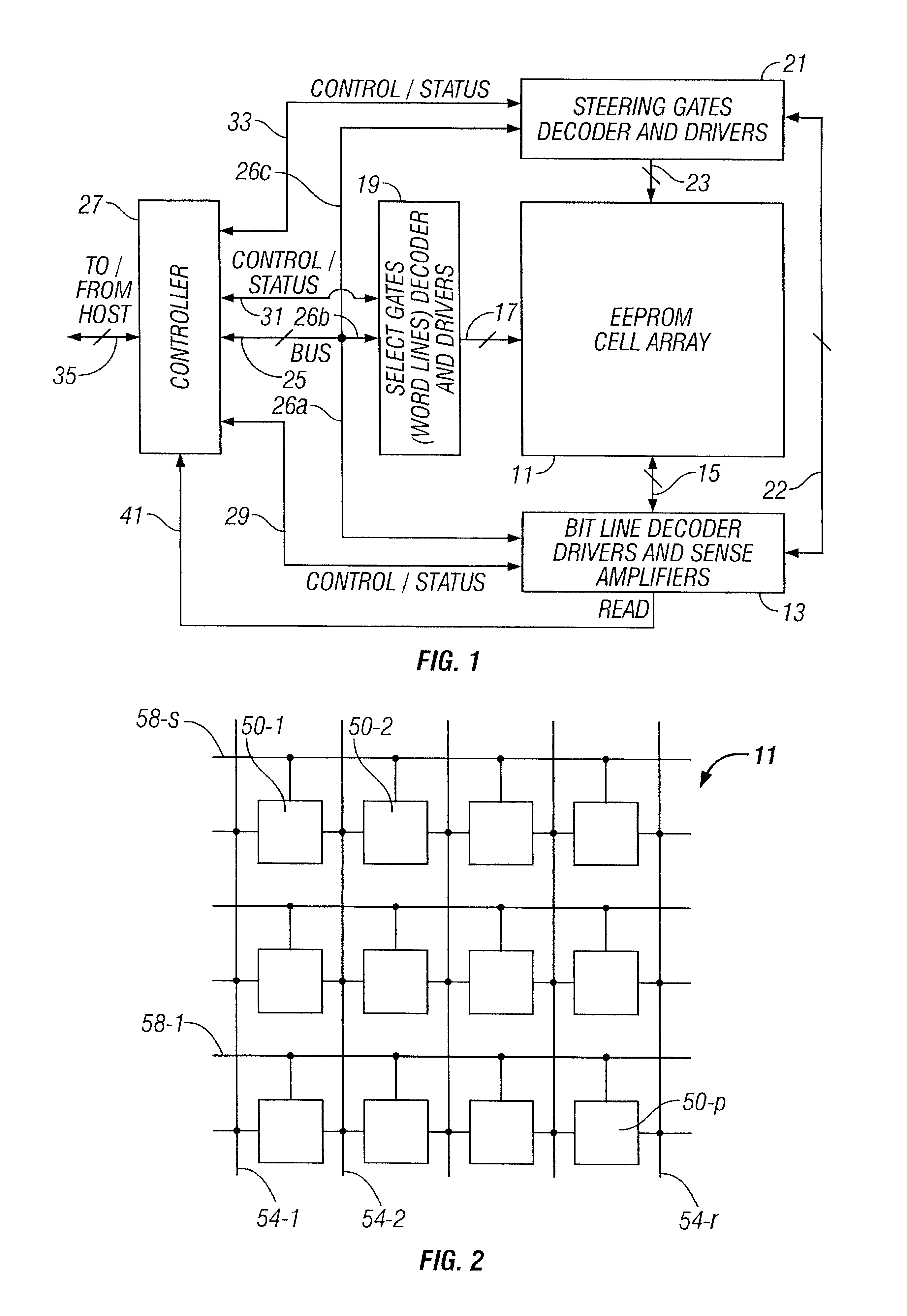
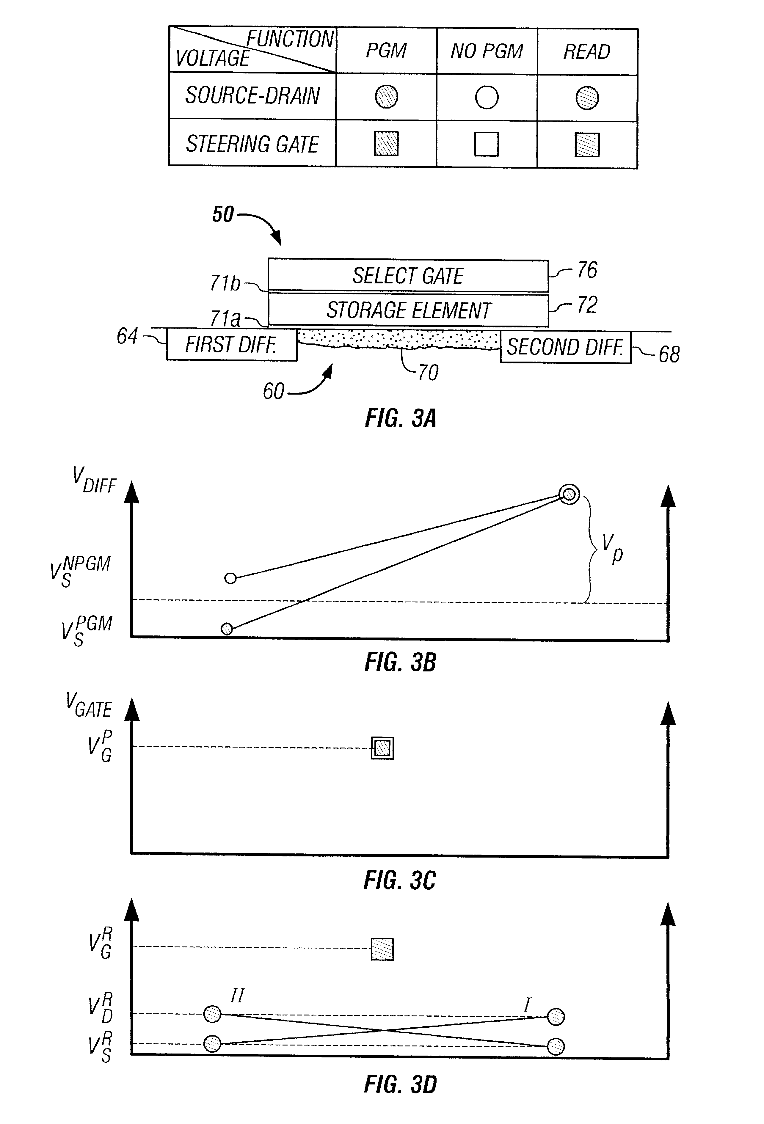
FIG. 1 shows a block diagram of a memory system controlling and driving an array of memory elements. A large number of individually addressable memory cells 11 are arranged in a regular array of rows and columns. Individual memory cells can be controlled by bit lines, s elect gates and steering gates. Bit lines are designated herein to extend along columns of array 11, and word lines are designated to extend along the rows of array 11. Bit line unit 13 may include a bit line decoder, storage elements, driver circuits and sense amplifiers. Bit line unit 13 can be coupled to cell array 11 by line 15, and to controller 27 by bit-control line 29 and by read line 41. Word line unit 19 may include a select gate decoder and driver circuits. Word line unit 19 can be coupled to cell array 11 by line 17, and to controller 27 by word-control line 31. Steering line unit 21 may include a steering gate decoder and driver circuits. Steering unit 21 can be coupled to cell array 11 by line 23, to co...


PUM


Abstract

The cells of a memory cell array are programmed in a pair wise manner. The pairs are separated by at least one memory cell, reducing the possibility of interference between the pairs during programming. The memory cells are programmed individually by applying a relatively high voltage to one of the bit lines of each cell regardless whether the cells are to be programmed or not, while applying a lower voltage to the second bit lines, depending on whether the cells are to be programmed or not. This programming voltage assignment enhances the speed of programming. Furthermore, the pair wise programming scheme applies the necessary high voltages only half as often as in previous schemes to program all the cells of the array, increasing the lifetime of the memory system.

Description

1. Field of InventionThe invention relates to programming floating gate memory cells, and in particular to improved techniques of reading and writing of dual floating gate memory cells.2. Discussion of Related ArtThere are many commercially successful non-volatile memory products being used today, particularly in the form of small cards, which use an array of flash EEPROM cells. The basic architecture of an individual EEPROM memory cell includes source and drain diffusions, coupled by a channel, formed in a semiconducting substrate. The storage element itself is positioned above the channel, separated from it by a dielectric layer. This storage element is often referred to as a floating gate. Overlying the storage element there can be a select gate, used to address the individual cell for programming and reading.Some designs include a split channel architecture, as described, for example, in U.S. Pat. No. 5,095,344, granted to E. Harari, which is incorporated herein by this referenc...

Claims


Application Information

Patent Timeline
Patent Type & Authority Patents(United States)
IPC IPC(8): G11C16/06G11C16/10G11C16/26G11C16/04G11C16/02H01L21/8247H01L27/115H01L29/788H01L29/792
CPCG11C16/10G11C16/26G11C16/0491G11C16/00
Inventor CERNEA, RAUL-ADRIAN
Owner SANDISK TECH LLC
Why Eureka
Try Eureka