

Self-aligned silicide (salicide) process for strained silicon MOSFET ON SiGe and structure formed thereby
a technology of strained silicide and strained silicide, which is applied in the direction of basic electric elements, electrical equipment, semiconductor devices, etc., can solve the problems of consuming some of the underlying sige, strained silicide is too thin to accommodate the conventional silicide, and the application of self-aligned silicide (salicide) process is not straightforward
- Summary
- Abstract
- Description
- Claims
- Application Information
AI Technical Summary
Problems solved by technology
Method used
Image

Examples
Embodiment Construction
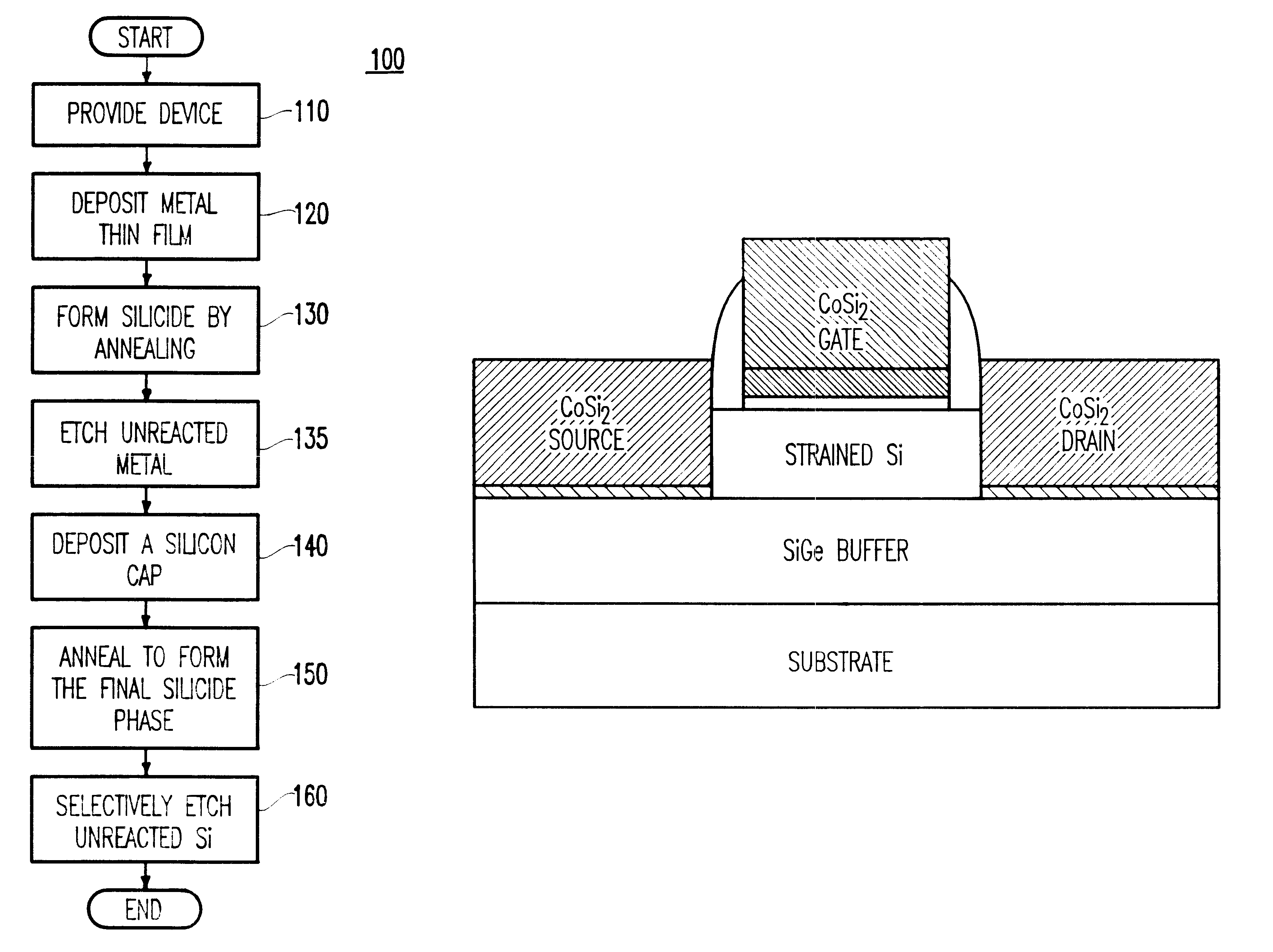
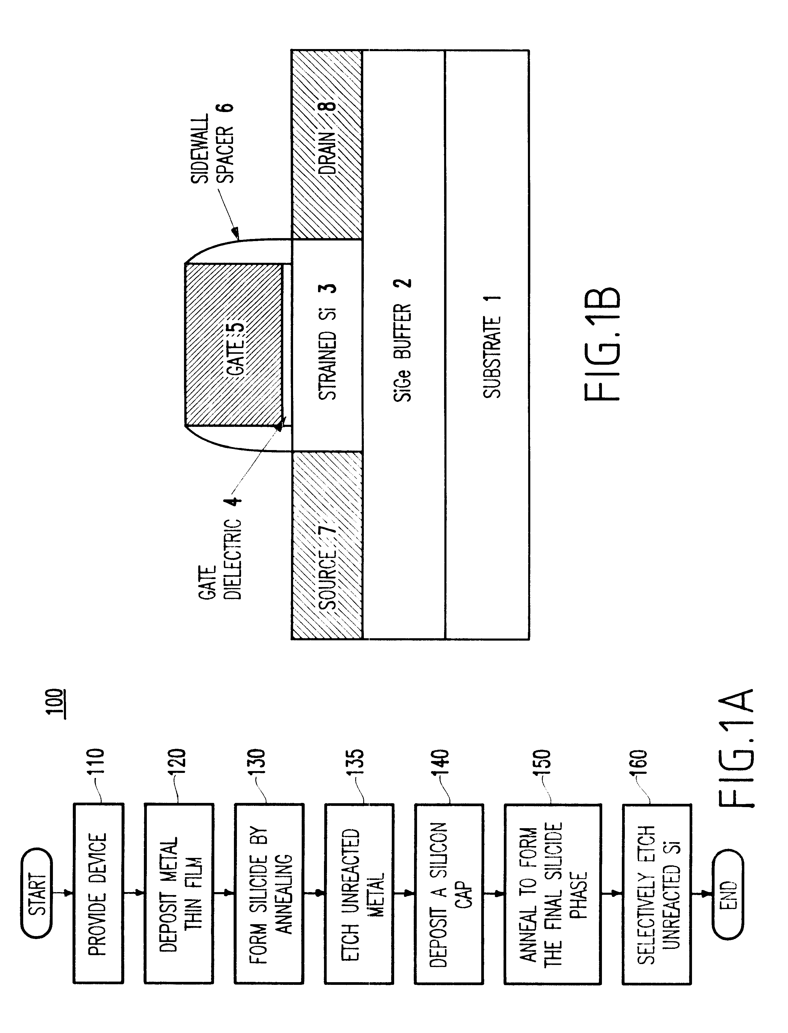
Referring now to the drawings, and more particularly to FIGS. 1A-7, there is shown a preferred embodiment of the method and structures according to the present invention.
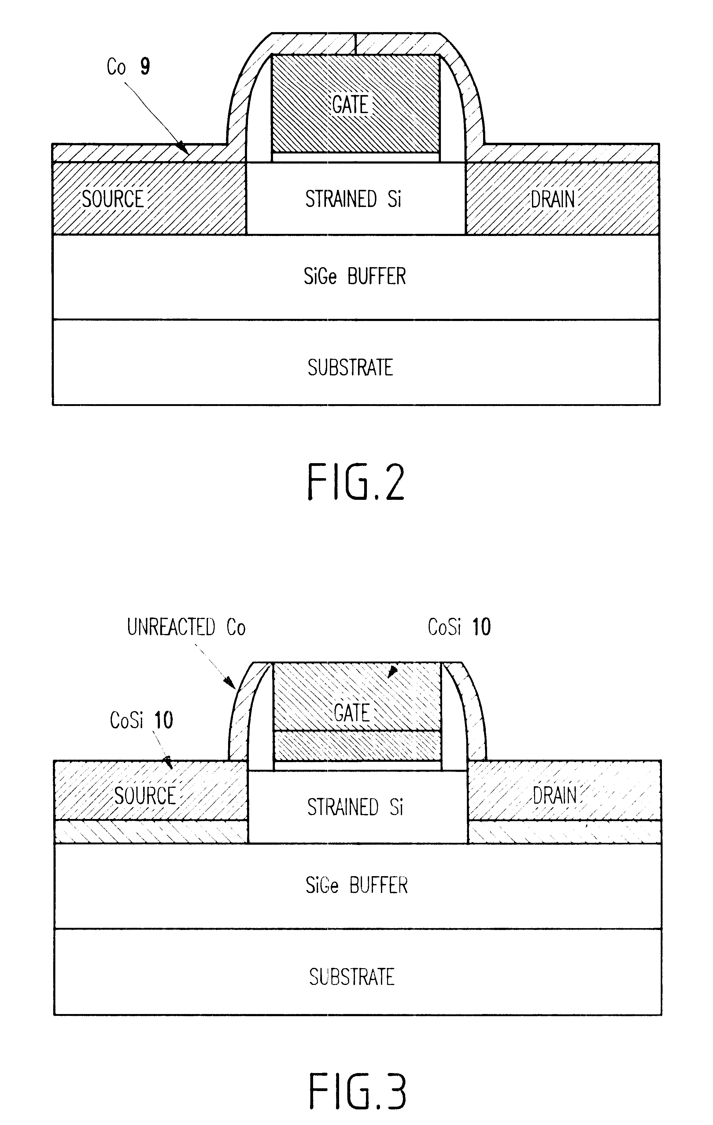
The process flow is shown in FIGS. 1A to 6. Although the process flow is demonstrated using a conventional MOSFET structure, the method of the present invention is applicable to almost any other, less frequently used, structures as well and such can be considered as a method of forming a substrate. Hereinbelow, the use of Co has been assumed, but other metals useful for suicides such as Ti, Pd, and / or Pt, also can be used with the present invention.
FIG. 1A illustrates a flow diagram of the inventive method 100, whereas FIGS. 1B through FIG. 6 show the structure processed by the inventive method.
FIG. 1B shows the initial device to be silicided (e.g., see step 110 of FIG. 1A). The structure includes a Si substrate 1, a "relaxed" SiGe buffer layer 2, a strained Si film 3, a gate dielectric 4, a patterned gate 5, and tw...
PUM
 Abstract
Description
Claims
Application Information