Integrated circuit partitioning placement and routing system

a technology of integrated circuits and routing systems, applied in computer aided design, program control, instruments, etc., can solve the problems of slow convergence of intensive iterative process, inability of designers to substantially modify logic modules within ic designs, and insufficient timing verification at this stage of design. achieve the effect of high accuracy

Inactive Publication Date: 2003-02-11
CADENCE DESIGN SYST INC
View PDF11 Cites 55 Cited by
  • Summary
  • Abstract
  • Description
  • Claims
  • Application Information

AI Technical Summary

Benefits of technology

to provide a placement and routing system that automatically produces initial floor and pin assignment plans that determines the appropriate size, shape, positions of circuit partitions with high accuracy so that a detailed placement and routing process can thereafter quickly optimize placement and routing of components forming the partitions.

Problems solved by technology

However timing verification at this stage of the design is still not entirely accurate since the netlist model does not take into account the actual physical layout on an IC chip of the cells that will form the circuit.
One undesirable effect of a divide-and-conquer placement algorithm is that it discards the hierarchical nature of the design and does not place the cells of any module in a well-defined area of an IC.
This makes it impossible for the designer to substantially modify a logic module within an IC design without repeating the placement and routing process for the entire IC.
However since the design engineer often does not have as much information on which to base the choice of partition shape, position and pin assignments, the initial shape, position and pin assignments for each partition are often based on little more than "educated guesses".
This labor intensive iterative process can be slow to converge to an acceptable IC layout, and the final layout my be less than optimal in many respects.

Method used


Image

  • Integrated circuit partitioning placement and routing system
  • Integrated circuit partitioning placement and routing system
  • Integrated circuit partitioning placement and routing system

Examples


Embodiment Construction

)

Modular Circuit Design

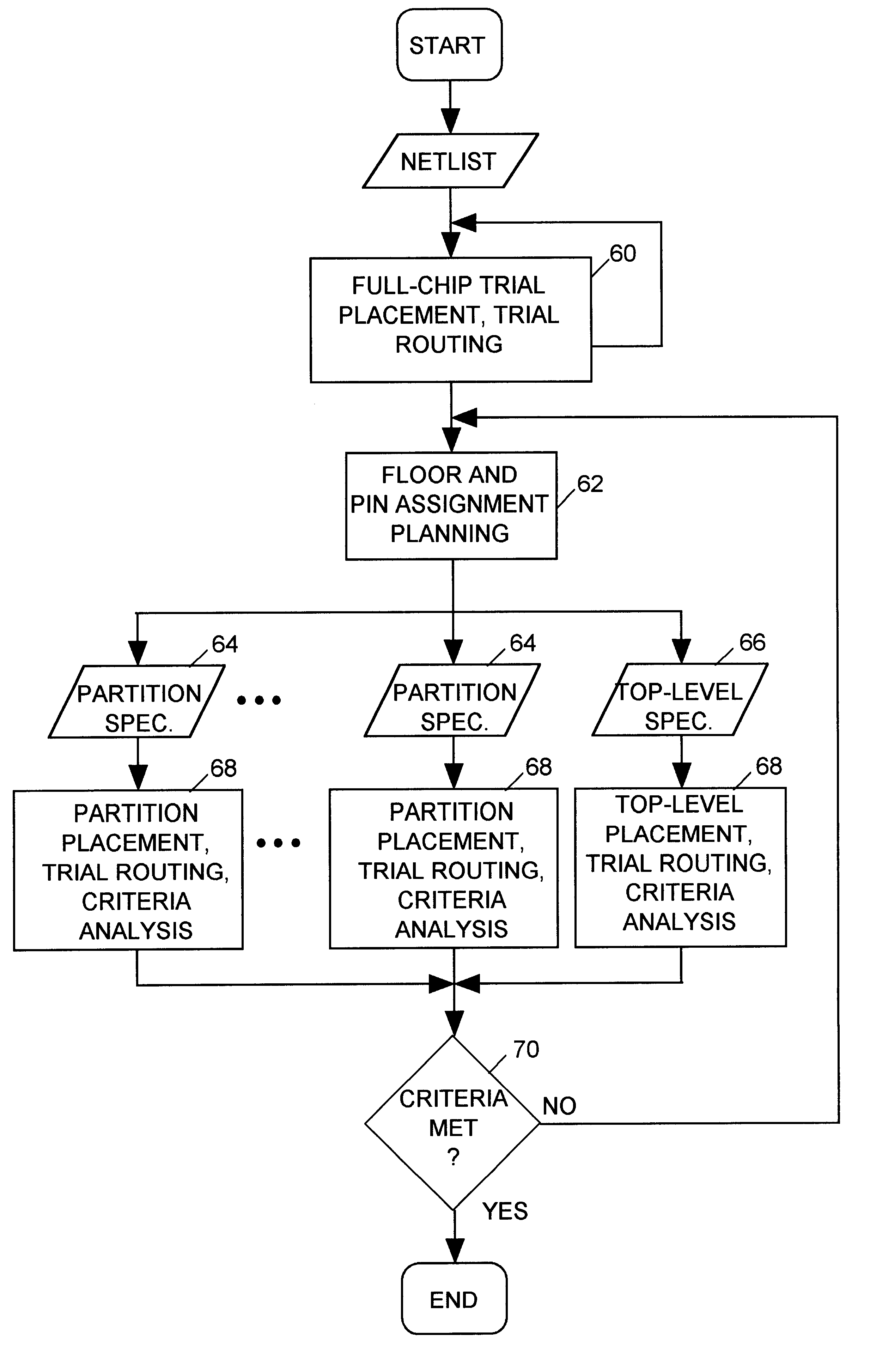
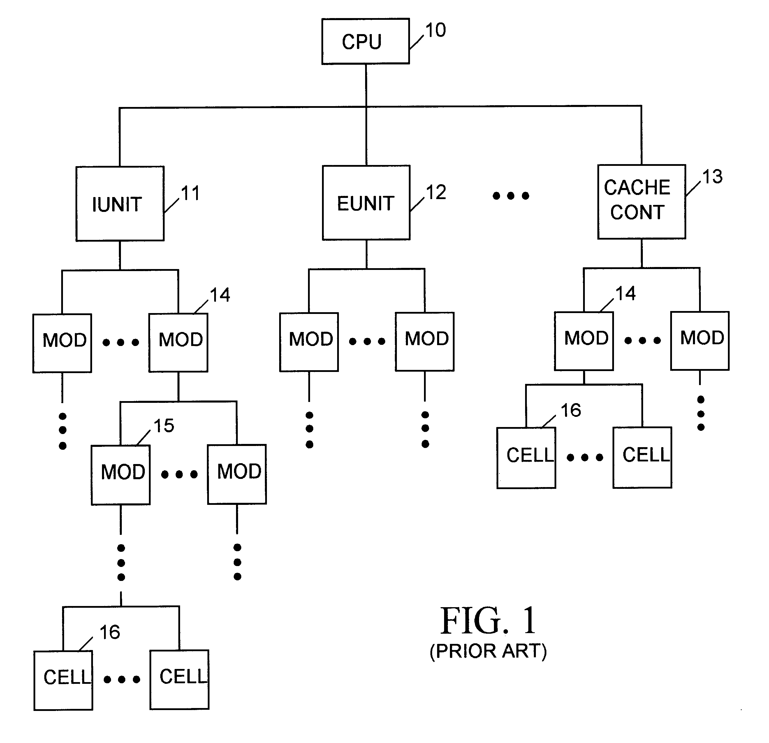
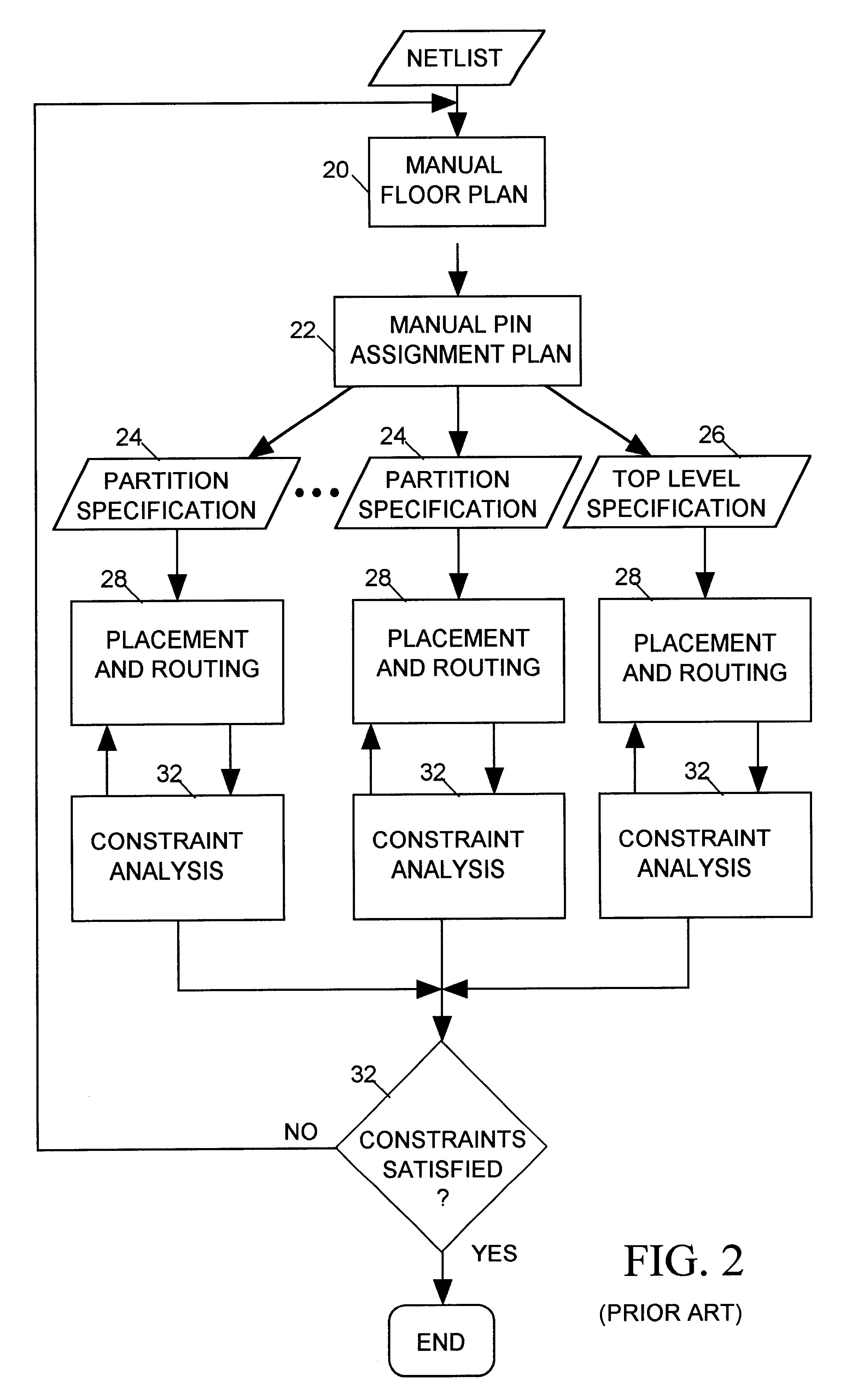
A placement and routing system in accordance with the invention processes a netlist or similar model of a circuit to determine a suitable layout for circuit components within an integrated circuit (IC) substrate. A netlist typically models an IC as a hierarchy of circuit modules wherein each higher level module is formed by lower level modules. FIG. 1 illustrates in block diagram form an example of a prior art hierarchical logic design of a central processing unit (CPU) 10 formed by several high level modules including for example an instruction unit (IUNIT) 11, an execution unit (EUNIT) 12, and a cache controller 13. Each high level module 11-13 is formed by several lower level modules 14 which in turn are formed by still lower level modules 15. Small circuit cells 16 such as logic gates and individual transistors form modules residing at the lowest levels of the hierarchy. The placement and routing system automatically divides the design into several "partit...


PUM


Abstract

Disclosed herein is a method for dividing an integrated circuit (IC) design into several circuit partitions, each including one or more circuit modules, and then separately carrying out placement and routing for each circuit partition, with each partition being implemented within a separate area of an IC substrate. The method initially generates a whole-chip trial placement that tends to cluster cells of each circuit module together. An IC substrate floor plan assigning modules to various partitions is prepared, with the size, shape and relative position of each partition being determined by size, shape and relative position of areas of the substrate occupied by those modules in the trial floor plan. A trial routing is also performed with information on which to base a pin assignment plan for each module. A detailed placement and routing process is then independently performed for each partition, with placement and routing of cells within each partition constrained by the floor plan and pin assignment plan.

Description

1. Field of the InventionThe invention relates to methods for designing integrated circuits, and particularly to a system for determining the physical placement and interconnection of components forming an integrated circuit.2. Description of Related ArtAn IC design engineer typically models a circuit using a hardware description language (HDL) to describe the behavior of the various components making up a circuit and the manner in which those components are interconnected. The design engineer then programs a circuit simulator to simulate circuit behavior based on the HDL circuit model. Since the HDL model is a relatively high level behavioral model of the circuit, the initial circuit simulation does not take into account the timing and other constraints of the semiconductor technology that will implement the IC,After verifying circuit logic, the design engineer usually employs computer-aided design and engineering tools to convert the high-level HDL circuit model into a lower-level...

Claims


Application Information

Patent Timeline
Patent Type & Authority Patents(United States)
IPC IPC(8): G06F17/50H01L21/82H01L21/822H01L27/04
CPCG06F17/5072G06F30/392
Inventor CHAO, PINGDAI, WEI-JINIGUSA, MITSURUKAO, WEI-LUNSHEN, JIA-JYE
Owner CADENCE DESIGN SYST INC
Why Eureka
Try Eureka