Staircase program verify for multi-level cell flash memory designs

a multi-level cell, flash memory technology, applied in static storage, digital storage, instruments, etc., can solve the problems of inability to reprogramme in practical matter, data stored in such memory devices are susceptible to power loss, and require constant ambient power, so as to achieve the effect of increasing the performance of program verification

Inactive Publication Date: 2003-03-25
MONTEREY RES LLC
View PDF7 Cites 165 Cited by
  • Summary
  • Abstract
  • Description
  • Claims
  • Application Information

AI Technical Summary

Benefits of technology

One example of the method for concurrently verifying the programming of MLC flash memory designs comprises the step of applying a single stepped voltage pulse to the MLC flash memory array. The stepped voltage pulse has an initial value within a range substantially equivalent to that necessary to read data from the highest programmable level of the MLC flash memory cell and preferably within a range to provide a read margin to compensate for functional variations and reliability concerns. Each subsequent voltage level of the stepped voltage pulse is within a range substantially equivalent to a voltage necessary to read data from the next lowest programmable level preferably within a range

Problems solved by technology

Such devices, however, require constant ambient power in order to retain the charge.
Therefore, the data stored in such memory devices are susceptible to power loss.
While conventional EPROM's provide reliable non-volatile storage, they typically may not be able to be reprogrammed in a practical matter.
In many applications, removing the memory is not practical to reprogram.
An EEPROM has the disadvantages of being expensive and having a relatively limited life span, according to the number of erased and write operations.
The SRAM offers high operating speeds but only maintains its ability to retain the information stored therein while power is supplied to it.
This necessitates additional hardware to maint

Method used


Image

  • Staircase program verify for multi-level cell flash memory designs
  • Staircase program verify for multi-level cell flash memory designs
  • Staircase program verify for multi-level cell flash memory designs

Examples


Embodiment Construction

Hereinafter embodiments of the present invention will be explained with reference to the accompanying figures.

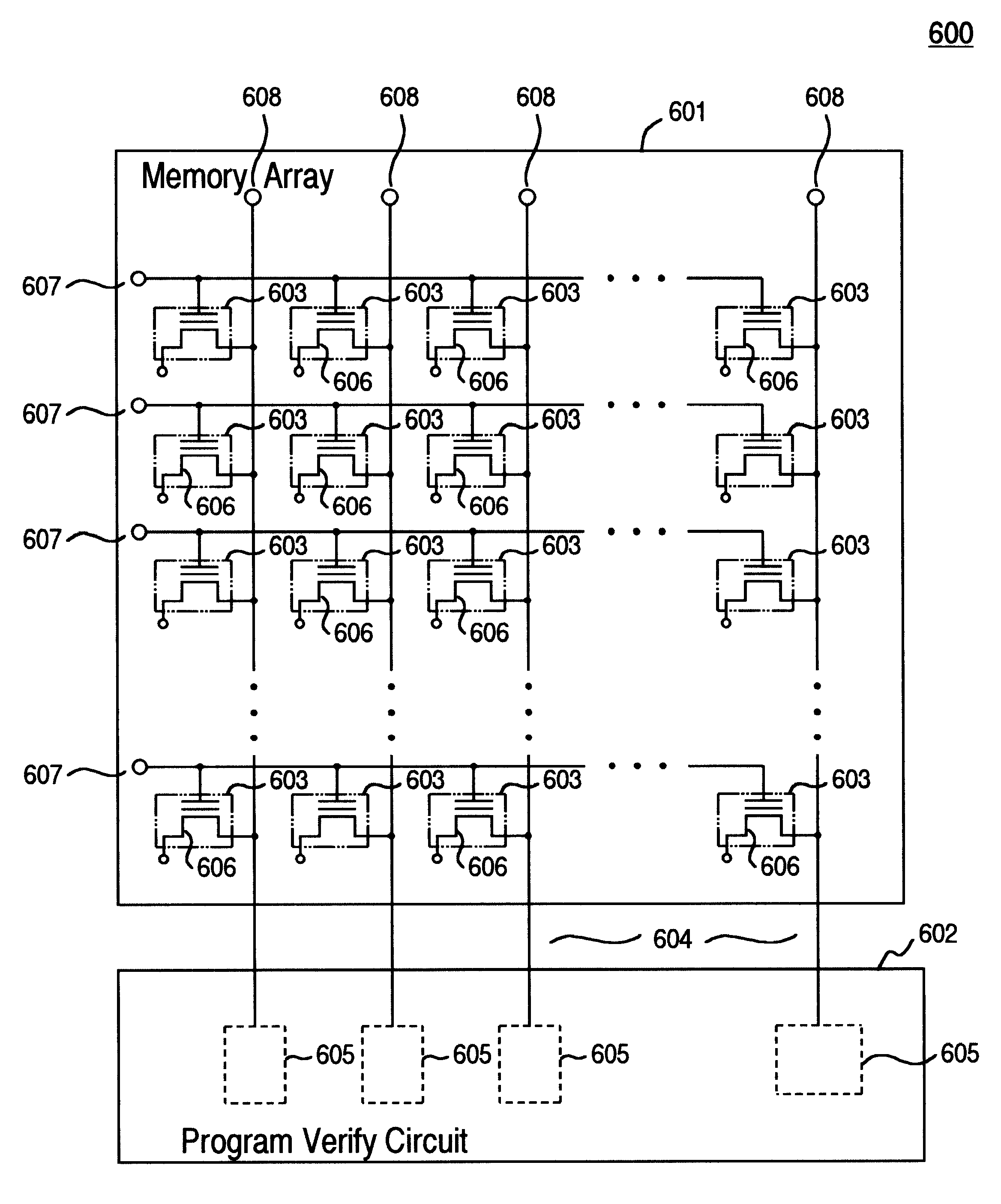
The illustrated embodiments provide system for program-verifying a multi-level-cell semiconductor memory device, commonly called a MLC flash memory device. An MLC flash memory device typically comprises an array of memory cells each having at least one storage element therein, the storage element configured to be programmed to store an N-bit combination of logical data, where N.gtoreq.2. The storage element, typically a transistor with a programmable threshold voltage V.sub.t, is configured to store the N-bit combination of logical data by programming the storage element to any one of 2.sup.N data storage levels. To ensure accurate programming of data in the memory array and to inhibit a properly programmed memory cell from subsequent programming, the data stored therein is program-verified. The principles of the present invention provide a system for reducing the time to pr...


PUM


Abstract

A system for concurrently verifying programming of logical data in a multi-level-cell (MLC) flash memory device having a plurality of memory cells each configured to store N bits of logical data where N>=2. The MLC flash memory device has a plurality of memory cells capable of being storing N-bits of data in one of 2N distinct data storage levels, each data storage level corresponding to a discrete N-bit combination of logical data. The data storage levels include a default level, called the erased level, and 2N-1 program levels, including a lowest program level, 2N-2 intermediate program levels and a highest program level. For each memory cell to be verified as programmed, an N-bit combination of data to be verified is loaded into a program-verify circuit and a stepped voltage pulse having 2N-1 steps is applied to each memory cell. The stepped voltage pulse includes an initial step, at least one intermediate step and a final step with the initial step substantially equal to a program-verify voltage for the highest program level of the MLC flash memory within a the highest program level, each successive intermediate step is substantially equal to a program-verify voltage corresponding to an intermediate program level and the final step of the voltage pulse is substantially equal to a program-verify voltage for the lowest program level. Concurrently with the application of the stepped voltage pulse to each memory cell, the data storage level is verified as substantially within a program level corresponding to the N-bit combination for the memory cell. Subsequent to verifying the data storage level for a memory cell, the verified memory cell is inhibited form further application of a program pulse.

Description

1. Field of InventionThe present invention relates generally to the field of electronic data storage devices. More particularly, the present invention relates to non-volatile multi-level-cell semiconductor memory devices and a method for reducing program-verify time in non-volatile multi-level-cell semiconductor memory devices.2. Description of Related ArtMany electronic devices, such as computers, personal digital assistants, cellular telephones, digital cameras and similar systems and devices include processors and memory fabricated from semiconductors. The memory is used to store computer programs to be executed by the device and / or data operated on by the processors to achieve the functionality of the device. Many devices and systems require that this information be retained in permanent storage--non-volatile medium--so that the data and computer programs remain when power is removed.Conventional semiconductor memory devices store bits of information in memory cells. The typical...

Claims


Application Information

Patent Timeline
IPC IPC(8): G11C16/06G11C11/56G11C16/34
CPCG11C11/5628G11C16/3468G11C16/3454G11C2211/5621
Inventor PARKER, ALLAN
Owner MONTEREY RES LLC
Why Eureka
Try Eureka