System for mapping logical functional test data of logical integrated circuits to physical representation using pruned diagnostic list

a technology of logical integrated circuits and diagnostic lists, applied in testing circuits, resistance/reactance/impedence, instruments, etc., can solve problems such as inability to "bitmap" the logic area of a chip, errors in read/write testing pin-point likely physical defects, and memory chips in reality lend themselves to failure analysis

Inactive Publication Date: 2003-04-22
HARRIS KAYOT +1
View PDF2 Cites 33 Cited by
  • Summary
  • Abstract
  • Description
  • Claims
  • Application Information

AI Technical Summary

Problems solved by technology

Failure analysis attempts to identify the cause of failure of chips of a particular chip design after the failures have been detected during production or prototype testing.
Memory chips in reality lend themselves to failure analysis because of their structure as regular arrays of memory cells.
The errors in read / write testing pin-point likely physical defects at readily identified location.
As a result of this identification, trouble-shooting would focus on the production process rather than the design of the part.
There has been no way to "bitmap" area of logic within a chip.
Furthermore, logic chip function test results do not provide a starting point for the physical coordinates of failures within a failed die.
However, even after a list of failing signals is produced for a given dies, it is still not possible to find the physical location of the failure because each failing signal may contain hundreds of transistors within its "cone of logic," and there are usually multiple failing signals.
This approach suffers from several drawbacks, including: the inability to relate a particular bin's fall-out to a suspect process level; the inability to distinguish pre-packaging yield issue from packaging yield issues; and the inability to establish a clear link between large populations of failed die.
For example, if a series of values is applied to the scan cells within the circuit such that the voltage value at a particular net should be at a high voltage level, but the voltage level at the particular net remains at a low voltage level, a stuck-at fault is detected.
Such flaws may include, but are not limited to, pin faults, element failures, metallization failures, improper metal oxidation, or incorrect ion implantation.
However, not all problems in a circuit can be detected using stuck-at fault testing models.
Stuck-at fault models may not present a design or manufacturing team with sufficient information to easily determine the causes of particular faults that are detected in a circuit.
Other faults, known as bridging faults, include faults that are the result of defects or failures involving more than one particular net.
For example, two metal leads within a particular circuit layer or in adjacent circuit layers may be shorted, causing a fault that may not be easily detected or diagnosed using a stuck-at fault model of testing.
The problem with this methodology is that the confidence level of the stuck-at diagnostic tools is only between fifty and seventy percent.

Method used


Image

  • System for mapping logical functional test data of logical integrated circuits to physical representation using pruned diagnostic list
  • System for mapping logical functional test data of logical integrated circuits to physical representation using pruned diagnostic list
  • System for mapping logical functional test data of logical integrated circuits to physical representation using pruned diagnostic list

Examples


Embodiment Construction

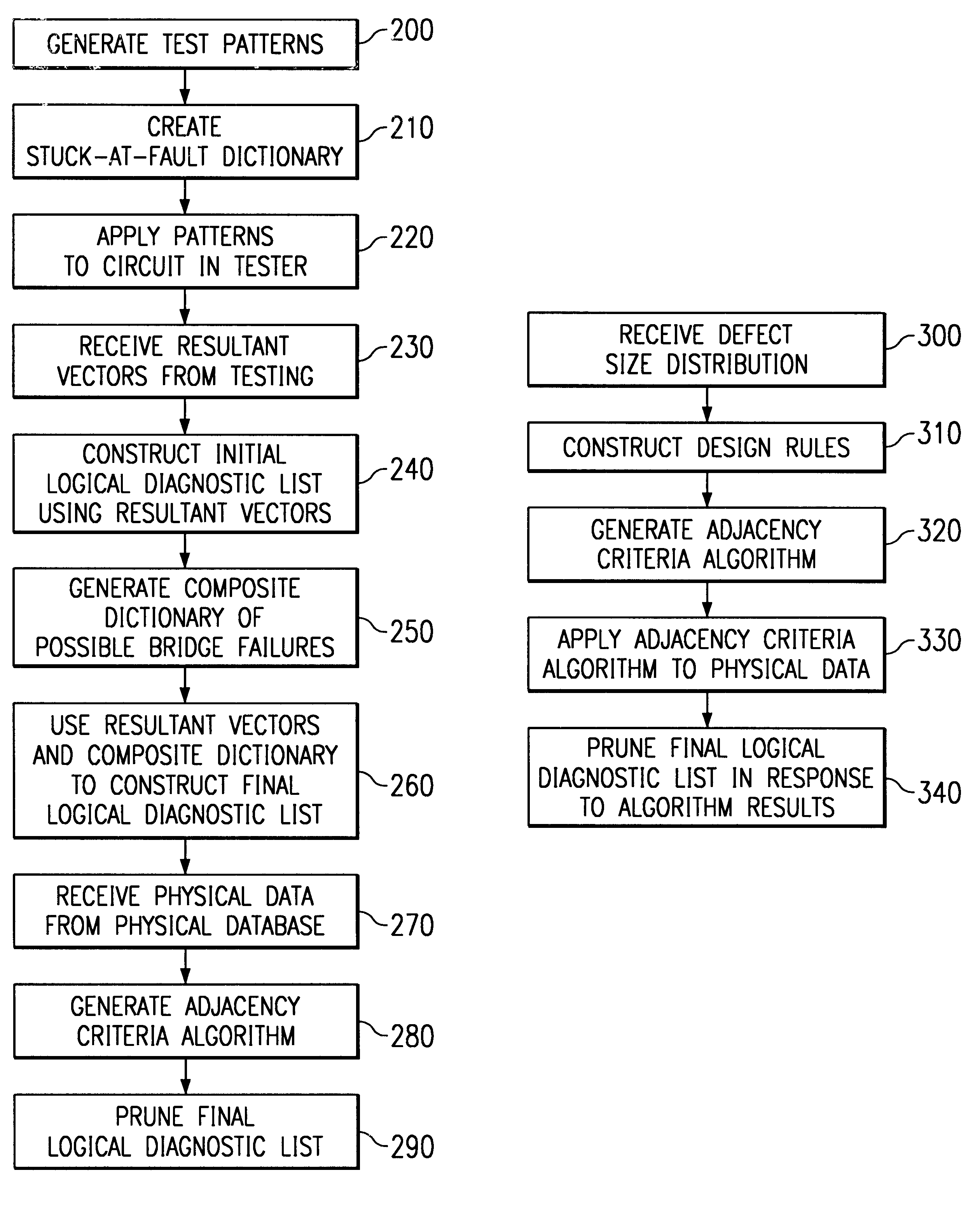
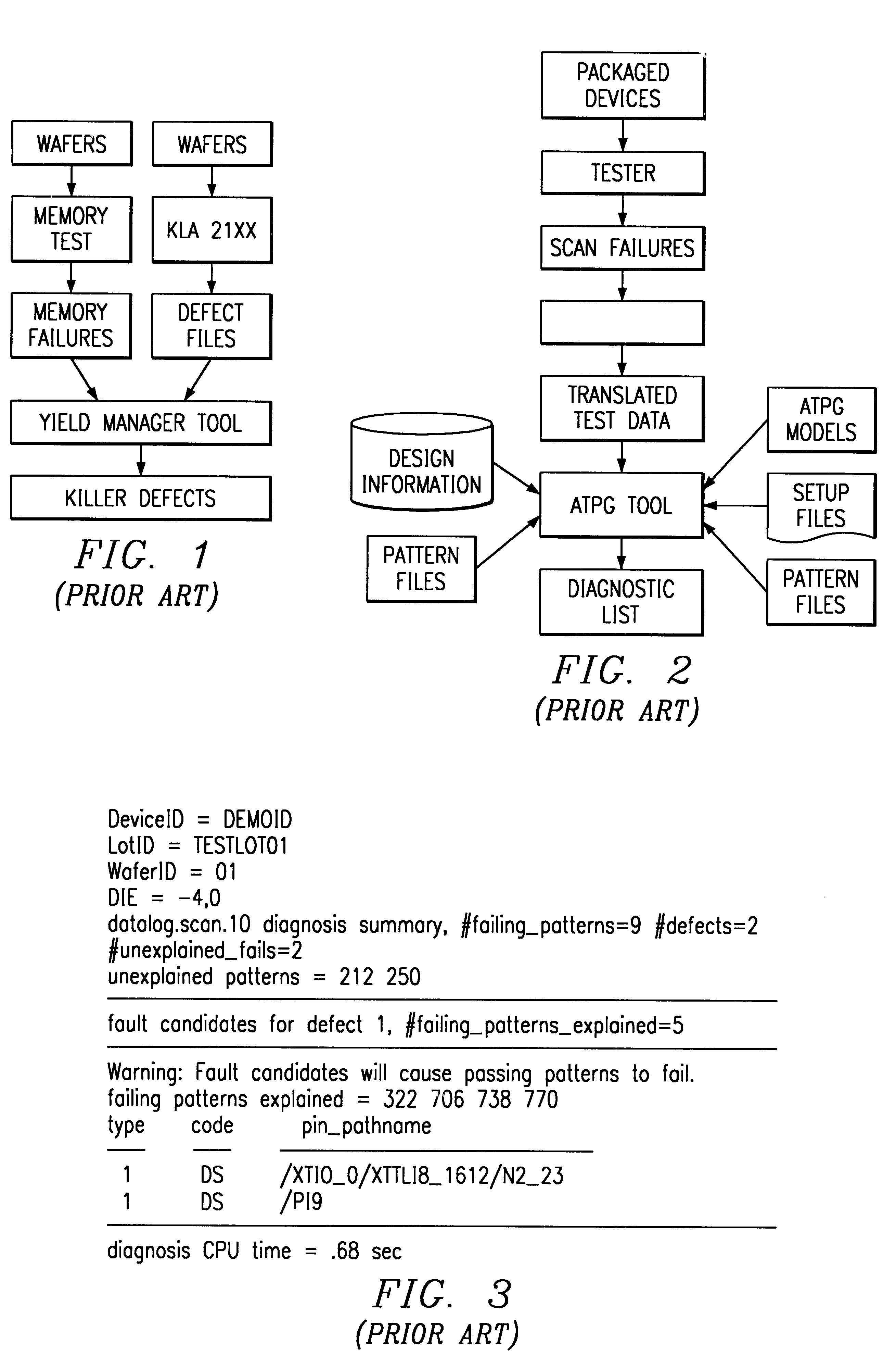
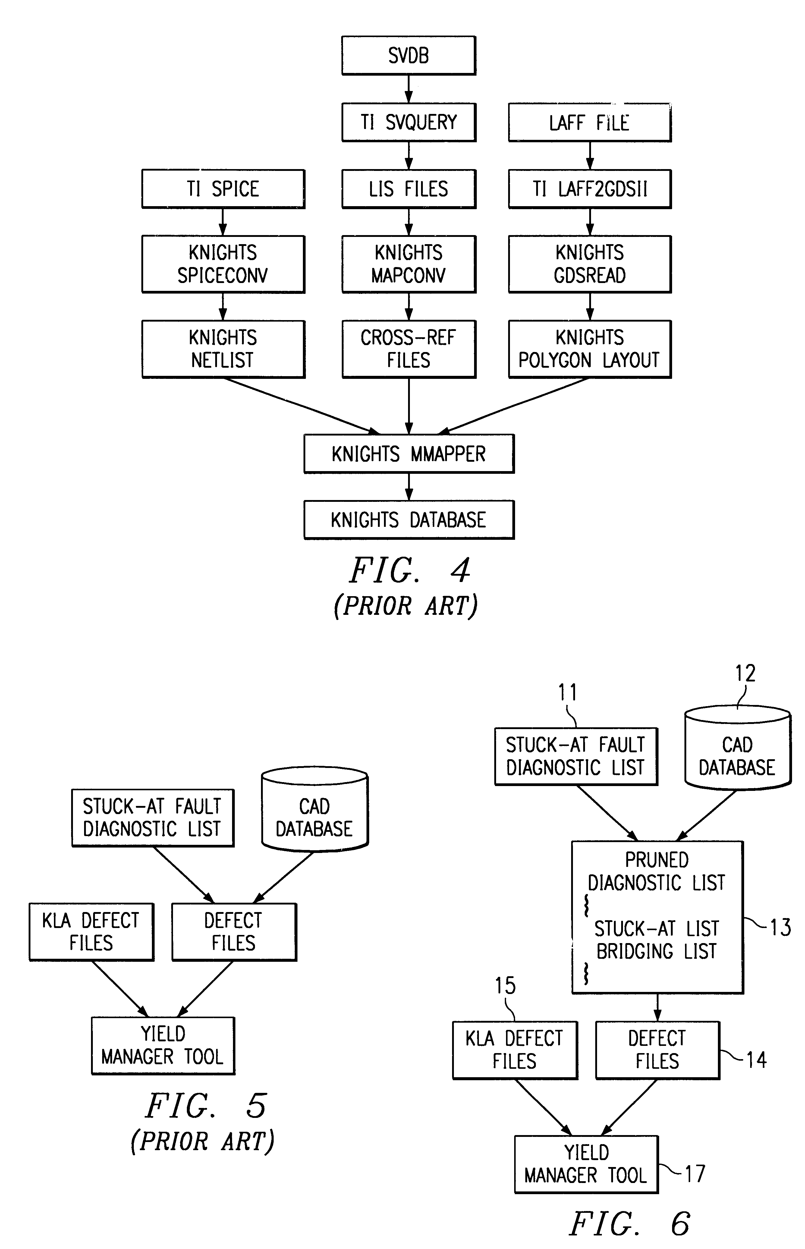
Referring to FIG. 5, there is illustrated the logic bitmap flow using stuck-at fault diagnostic list. The defects are collected using, for example, a KLA 21xx in-line manufacturing equipment. This is applied as one input to the Yield Management tool. The other input to overlay is provided by the stuck-at fault diagnostic list and the Computer Aided Design (CAD) database using a commercially available ATPG tool. The ATPG tool uses the translated test data, together with the test pattern files, set-up files, one or more ATPG diagnostic models, and design information from the design database to identify suspected failing nodes, output from the diagnostic list. For more information, refer to application Ser. No. 09 / 192,164, filed Nov. 13, 1998 of Shawn Smith, Hari Balachandran and Jason Parker entitled "IC Test Software System for Mapping Logical Functional Test Data of Logical Integrated Circuits to Physical Representation" incorporated herein by reference.

In accordance with the prefer...


PUM


Abstract

An improved method for mapping logical function test data of logical integrated circuits to physical representations uses a pruned diagnostic list. The steps include creating a final logical diagnostic list of potential bridging faults in response to testing the circuit for stuck-at faults at a plurality of nets of the circuit, receiving the physical data associated with nets of the circuit, applying adjacency criteria to the physical data, generating a pruned diagnostic list of potential bridging faults in response to applying the adjacency criteria, performing in-line inspection to obtain second localized probable defect data and correlating second localized portable defect data with the pruned diagnostic list.

Description

This invention relates to integrated circuit (IC) chip test software systems and more particularly to refining logic bitmap using pruned diagnostic list.BACKGROUND OF INVENTIONDigital semiconductor integrated circuits are manufactured on dies of a silicon wafer. There are both memory chips and logic chips. A microprocessor chip is an example of a logic chip. A field known as Design for Test (DFT) involves designing into the chip "scan chains" that are used to write and read portions of the chip that might be otherwise inaccessible. Layout tools are used to lay out a chip design onto the silicon wafer. The chip layout may be represented in the form of a netlist which is a bit of low-level design cells and the interconnections between them. Once the design is completed, the bits of a file representing the chip are written to a tape or disk. A mask maker makes photomasks to manufacture the chip using the files.The chips are production monitored and tested. Production monitoring is perf...

Claims


Application Information

Patent Timeline
Patent Type & Authority Patents(United States)
IPC IPC(8): G01R31/28G01R31/317
CPCG01R31/31704G01R31/2894
Inventor BALACHANDRAN, HARI
Owner HARRIS KAYOT
Why Eureka
Try Eureka