Method for forming a storage node of a capacitor

a technology of capacitors and storage nodes, which is applied in the field of capacitors, can solve the problems of reducing the electrical characteristics of capacitors to be degraded, increasing the number of unit processes, and complicated processes, and achieves the effects of improving the electrical characteristics of semiconductor products, simplifying the fabrication process, and fine line width

Inactive Publication Date: 2003-05-13
INTERLOTT TECH +1
View PDF5 Cites 24 Cited by
  • Summary
  • Abstract
  • Description
  • Claims
  • Application Information

AI Technical Summary

Benefits of technology

A method for forming a storage node of a capacitor which simplifies the fabrication process, and improves the electrical characteristics of semiconductor products by forming the storage node of a capacitor with no stepped portion between cell regions and peripheral circuit regions necessary for memory storage of next generation semiconductor products to which a fine line width is applied, and, at the same time, forming a guard ring for dividing the cell regions and the peripheral circuit regions.
The thickness of the storage node is formed less than about 1000 .ANG. to prevent shorting in a cylindrical cylinder.

Problems solved by technology

Thus, in case of increasing the size thereof, from the point of view of obtaining an etching selectivity, a cracking problem results due to a stress on a wafer.
If a thinner nitride film is used in order to avoid cracking, the nitride film gets attacked because of deficiency in a selection ratio in the dry etching of the capacitor oxide film, and even an inter-layer insulating film (ILD2) at lower portions is etched in the subsequent etching of the nitride film to thus become a leakage source, thereby causing the refresh characteristics of the capacitor to be degraded.
Hence, the number of unit processes is increased, and the processes become complicated, for thereby increasing production costs.

Method used


Image

  • Method for forming a storage node of a capacitor
  • Method for forming a storage node of a capacitor
  • Method for forming a storage node of a capacitor

Examples


Embodiment Construction

A preferred embodiment of the disclosure will now be described with reference to the FIGS. 1-7.

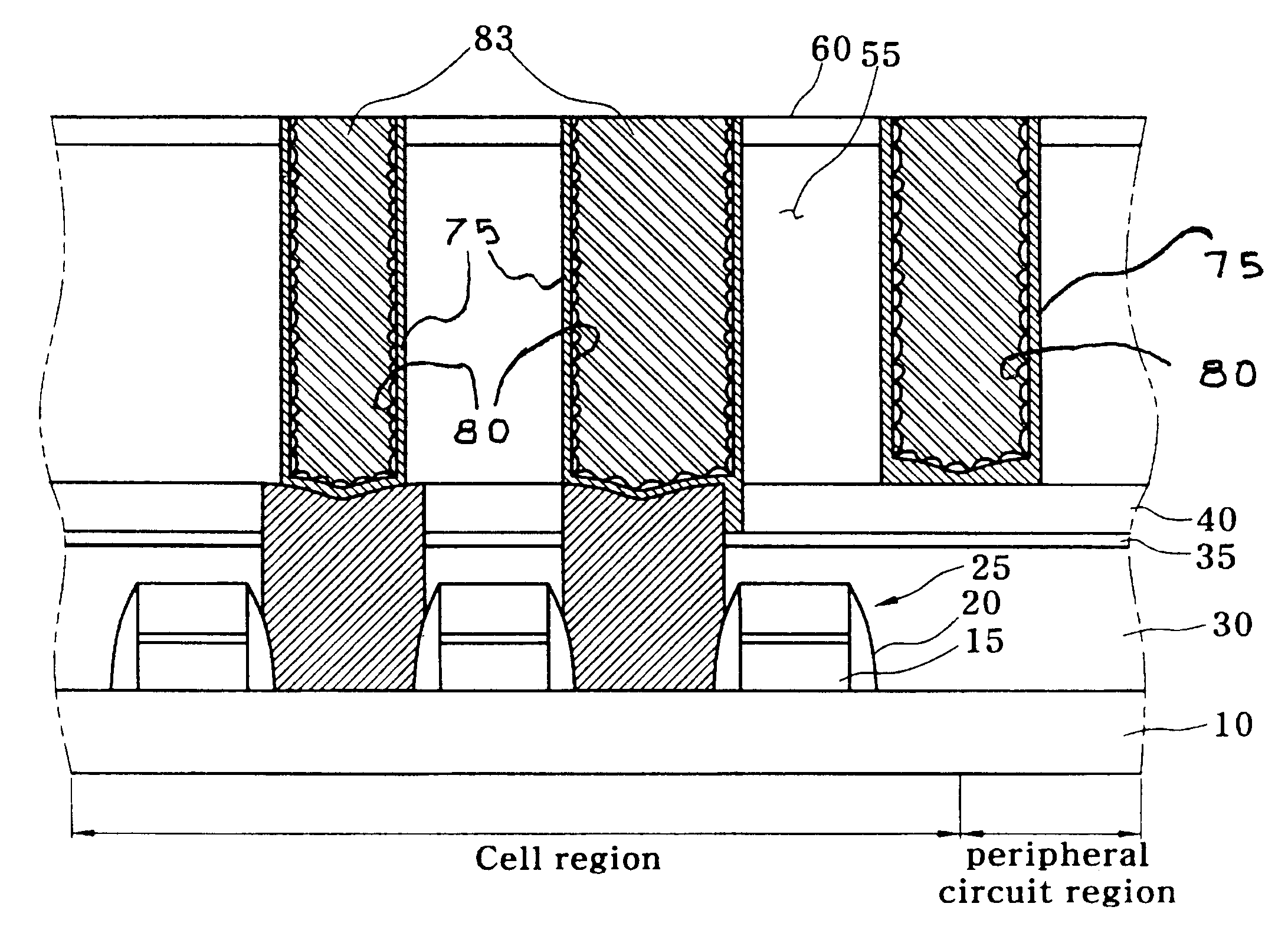
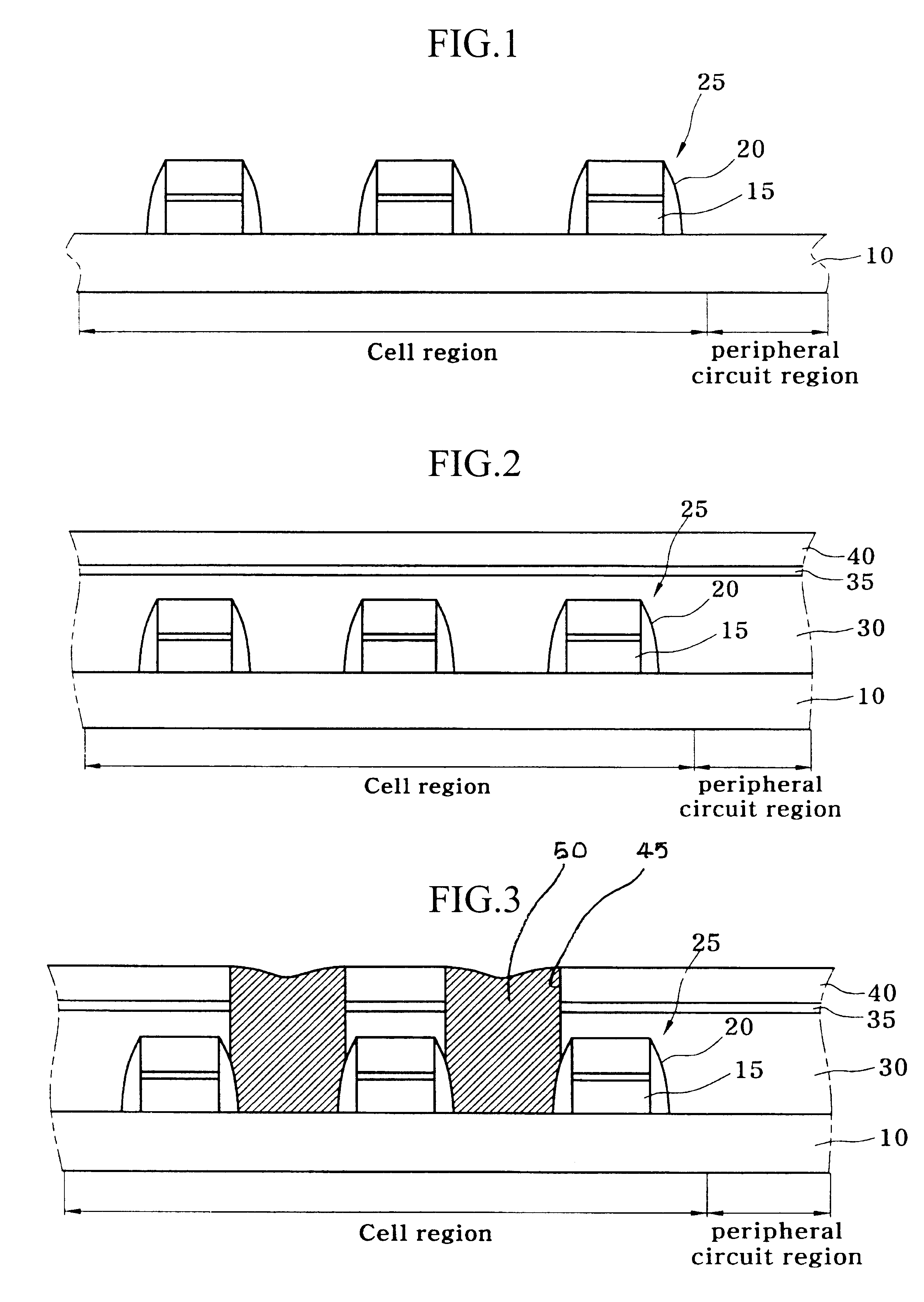
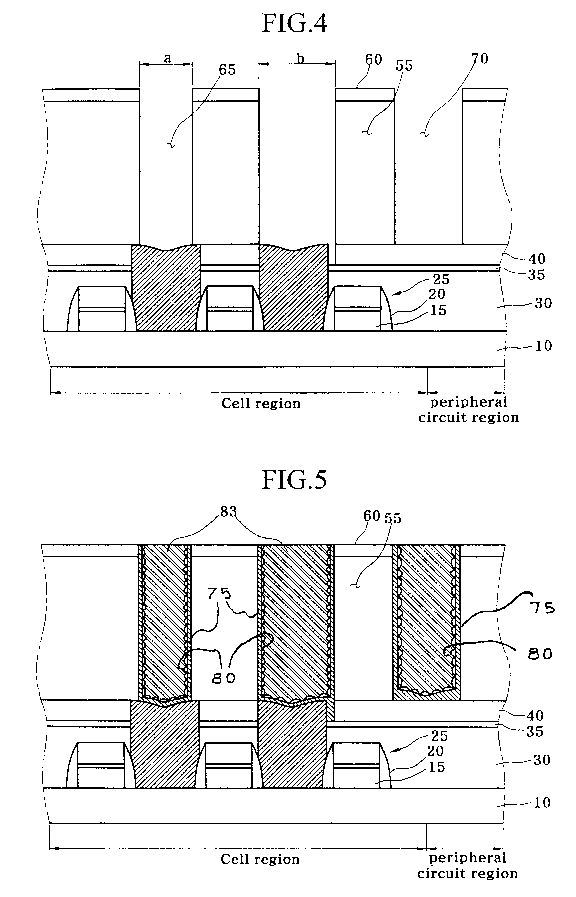
As illustrated in FIG. 1, a gate 25 having a bit line 15 and a spacer 20 are formed in a cell region of a semiconductor substrate 10.

Then, as illustrated in FIG. 2, an inter-layer insulating films 30, 40 and a barrier nitride film 35 are formed on the resultant material.

The barrier nitride film 35 is formed at a thickness ranging from about 200 to about 1500 .ANG. by the LP-CVD method and the PE-CVD method.

Then, as illustrated in FIG. 3, a contact hole 45 is formed on the resultant material by depositing a contact mask thereon and etching it. Thereafter, a polysilicon plug 50 is formed inside the contact hole 45 by depositing doped polysilicon therein and planarizing it by a polishing process.

When the barrier nitride film 35 and the first and second inter-layer insulating films 30 and 40 are dry etched, they are over-etched to about 30% of the thickness thereof.

Upon forming the polysilicon...


PUM


Abstract

A method for forming the storage node of a capacitor which simplifies its process, and improves the electrical characteristics of semiconductor products by forming the storage node of a capacitor with no stepped portion between cell regions and peripheral circuit regions necessary for memory storage of semiconductor products of the next generation to which a fine line width is applied, and, at the same time, forming a guard ring for dividing the cell regions and the peripheral circuit regions.

Description

1. Technical FieldA capacitor, and more particularly, a method for forming the storage node of a capacitor are disclosed. The disclosed method simplifies the fabrication process, and improves the electrical characteristics of the semiconductor product by forming the storage node of the capacitor with no stepped portion between cell regions and peripheral circuit regions necessary for memory storage of semiconductor products of the next generation to which a fine line width is applied, and, at the same time, forming a guard ring for dividing the cell regions and the peripheral circuit regions.2. Description of the Related ArtGenerally, a capacitor is the part storing a charge and supplying the charge necessary for the operation of a semiconductor device. As a semiconductor device is being highly integrated, the size of unit cells is being decreased, and the capacitance needed for the operation of the device is being increased little by little. The capacitance needed by devices of mor...

Claims


Application Information

Patent Timeline
Patent Type & Authority Patents(United States)
IPC IPC(8): H01L21/70H01L21/8242H01L21/02H01L27/108
CPCH01L27/10894H01L27/10852H01L28/91H01L28/84H10B12/033H10B12/09H10B12/00
Inventor LEE, KEE-JEUNGLEE, SEOUNG-WOOKLEE, SEUNG-HYUKKIM, CHAN-BAELEE, WAN-GIE
Owner INTERLOTT TECH
Why Eureka
Try Eureka