Field programmable optical arrays

a field-programmable, optical array technology, applied in multiplex communication, pulse technique, instruments, etc., can solve the problems of low power, etc., and achieve the effect of low power, high speed and low power

Inactive Publication Date: 2003-06-24
XILINX INC
View PDF9 Cites 38 Cited by
  • Summary
  • Abstract
  • Description
  • Claims
  • Application Information

AI Technical Summary

Benefits of technology

According to the invention, an FPGA-like architecture uses data paths formed almost entirely of optical switches and optical channels, and control of the switches using electrical signals. This combination makes for both high speed data transmission and highly flexible configuration.
According to the invention, the lookup table accesses optical signals (in one embodiment, a lookup table includes 16 switches for accessing optical signals, and one of the switches is selected by four input signals). The four input signals are electrical signals generated by optical signals. The four input signals route one of the 16 optical signals to an output terminal where it can be routed along a wave guide or through further optical switches to a final destination. Because most of the data path is optical, speed is high, power is low, and power loss is low.
It is estimated that a large improvement in speed will be available with this optical FPGA architecture. The speed of an electrical signal in an integrated circuit wire is on the order of 5 mm / ns. The speed of light in a waveguide (about half the speed of light in a vacuum) is on the order of 150 mm / ns. Instead of all FPGA signals being electrical, only the signals that control other signals must be electrical, therefore the overall speed is much faster.

Problems solved by technology

Because most of the data path is optical, speed is high, power is low, and power loss is low.

Method used


Image

  • Field programmable optical arrays
  • Field programmable optical arrays
  • Field programmable optical arrays

Examples


Embodiment Construction

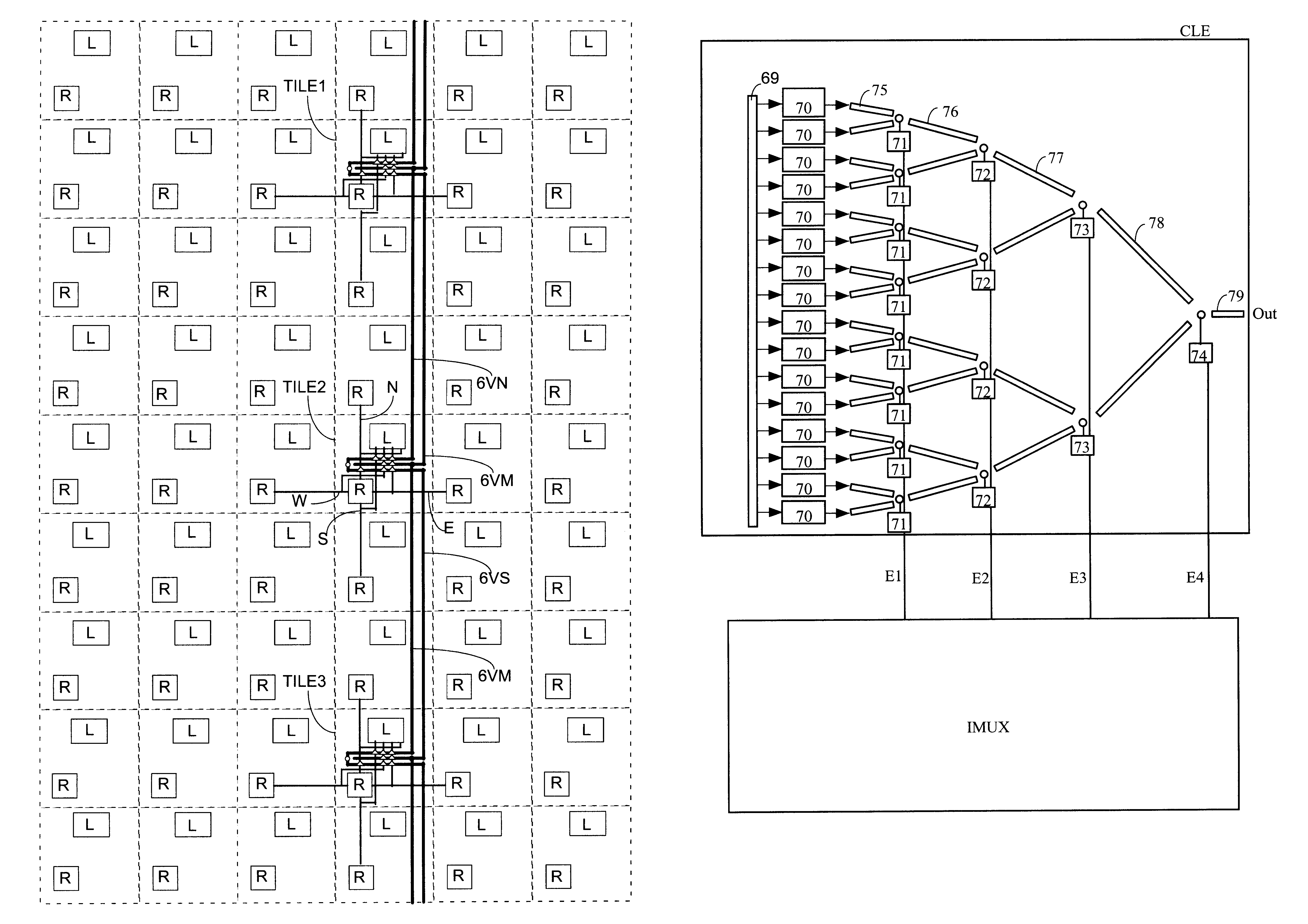
FIG. 5 shows a block diagram of an FPGA structure with which the present invention may be used. Each tile includes a logic structure L and a routing structure R. Also included, though shown for only a few tiles, is an interconnect structure by which one tile can be connected to another tile. The interconnect structures are the same for all tiles, as further discussed by Young et al. in U.S. Pat. No. 5,914,616, incorporated herein by reference. According to the current invention, the routing structures and the interconnect lines are optical and are programmably connected together by optical switches that are electrically controlled. The logic structures L include both electrical and optical connections, and are discussed in more detail in connection with FIGS. 6 and 7.

FIG. 6 shows in more detail one of the tiles of FIG. 5. The lines shown in FIG. 6, for example lines E, HE, LHE, VS, S, and LVS are all optical, and all switching that occurs in the structure labeled ROUTING (labeled R ...


PUM


Abstract

An FPGA is described using optical waveguides for routing signals through the FPGA. The routing is controlled electrically. Either coupling waveguides or resonant disks can be used for routing the optical signals. Lookup tables convert optical input signals to electrical signals for selecting values in the lookup table.

Description

FIELD OF THE INVENTIONThe present invention relates to semiconductor integrated circuit devices, more particularly to forming a field programmable gate array using optical signals and optical switches rather than or in combination with electrical signals and electrical switches.BACKGROUNDAs field programmable logic devices have become larger and more complex, there has been continuing demand for faster and lower power processing of signals. Until the present, the internal signals in a field programmable integrated circuit device as well as many other integrated circuit devices have been electrical signals carried by conductive metal or polysilicon lines. Transmission speed of these electrical signals is considerably slower than the speed of light. Thus, theoretically, the transmission speed can be increased.A good overview of the state of the art of optical networking technology and components is provided by the textbook authored by Ramaswami and Sivarajan titled "Optical Networks: ...

Claims


Application Information

Patent Timeline
Patent Type & Authority Patents(United States)
IPC IPC(8): G02B6/35
CPCG02B6/3508G02B6/3536G02B6/3556
Inventor BENNETT, DAVID W.MOHAN, SUNDARARAJARAOWITTIG, RALPH D.
Owner XILINX INC
Why Eureka
Try Eureka