Check patentability & draft patents in minutes with Patsnap Eureka AI!

Synchronous semiconductor memory device

a semiconductor and memory device technology, applied in the direction of information storage, static storage, digital storage, etc., can solve the problems of deterioration of characteristics, large noise generation, and relatively large sensing margin

Inactive Publication Date: 2003-07-22
KK TOSHIBA
View PDF8 Cites 21 Cited by
  • Summary
  • Abstract
  • Description
  • Claims
  • Application Information

AI Technical Summary

Problems solved by technology

In recent years, it is an important issue in the quest for faster semiconductor systems to increase the data transmission rate between a CPU and a semiconductor memory device.
Since a sense amplifier consumes considerable current for the purpose of amplifying a very small differential voltage, a number of the sense amplifiers tend to function as a problematic noise source when they are activated at the same time as described above.
This kind of power source noise may cause of malfunction and tends to degrade the sensitivity of the sense amplifier itself, resulting in deterioration in the characteristics thereof.
Namely, in accordance with the conventional semiconductor memory device supporting the double data rate mode, there is a problem that substantial noise is generated by simultaneously activating double the number of the sense amplifier as compared with that with the number of sense amplifiers activated during a conventional memory operation.
Also, in the sense amplifier serving to sense and amplify data to be outputted when the clock signal is pulled up, the interval between the time point at which the address becomes ready and the time point at which the sense amplifier enabling signal is given is elongated, as compared with the case where the sense amplifier serves to sense and amplify data to be outputted when the clock signal is pulled up, resulting in a relatively large margin for sensing and therefore resulting in a noise proof structure.

Method used


Image

  • Synchronous semiconductor memory device
  • Synchronous semiconductor memory device
  • Synchronous semiconductor memory device

Examples


first embodiment

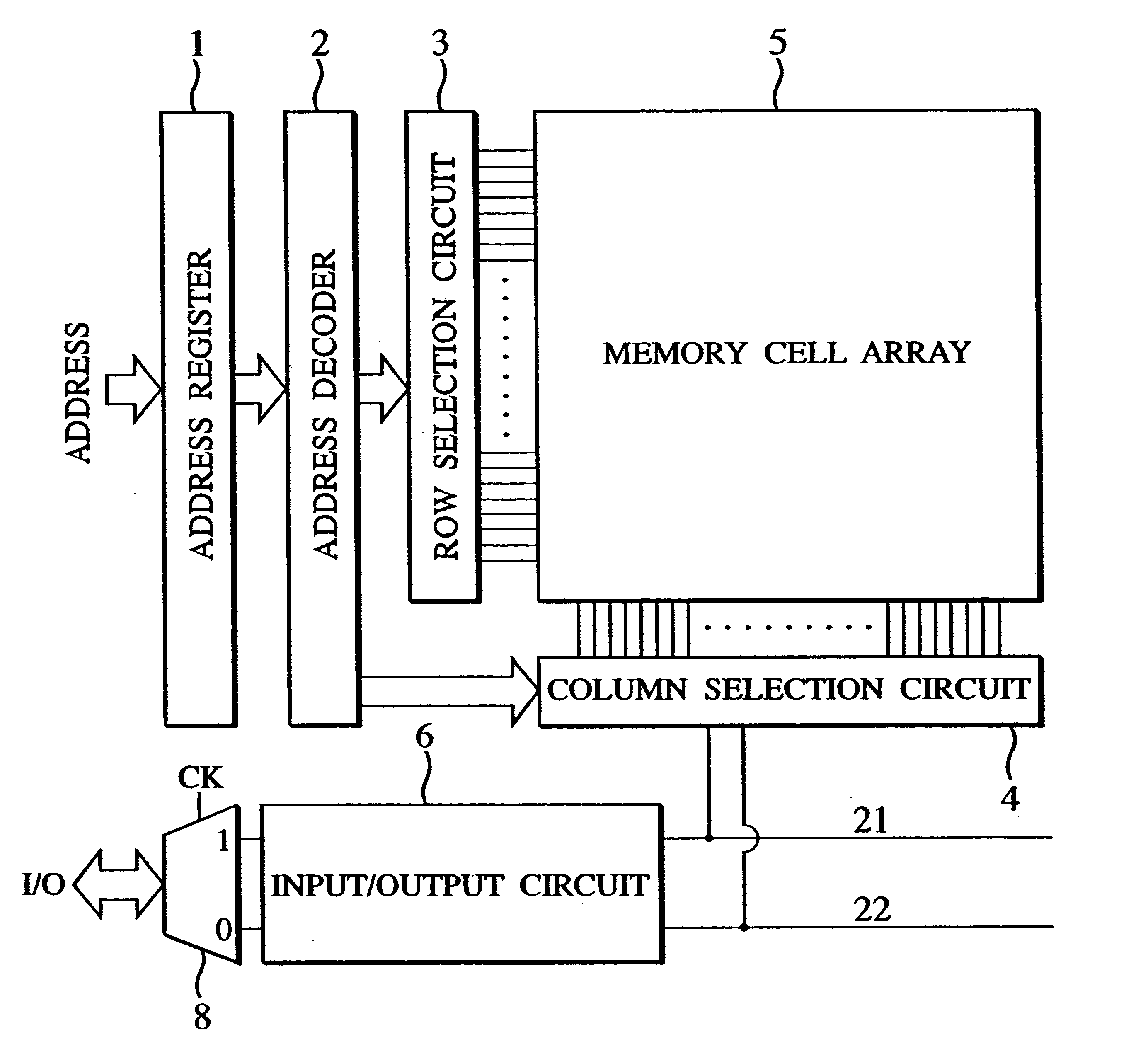
Several preferred embodiments of the invention will now be described in conjunction with the accompanied drawings. FIG. 4 is a block diagram showing a semiconductor memory device supporting the double data rate mode in accordance with the present invention.

The semiconductor memory device is composed of a memory cell array 5 having a number of memory cells, an address register 1, an address decoder 2 for receiving and decoding an address as latched by the address register 1, a row selection circuit 3 receiving from the address decoder 2 a row address signal for selecting a row of the memory cell array 5, a column selection circuit 4 receiving from the address decoder 2 a column address signal for selecting a column of the memory cell array 5, a data bus 21, a data bus 22, an output control unit 6 and a multiplexer 8. The row selection circuit 3 and the column selection circuit 4 serve to select two memory cells for one I / O terminal in accordance with the address signals as decoded.

Th...

second embodiment

FIG. 10 is a circuit diagram showing the configuration, inclusive of an exemplary circuit, of the output registers 62 and 64 in accordance with the present invention. The output register is composed of a master latch and a slave latch. Each latch is composed of clocked inverters 41 and 42 and an inverter 43.

In accordance with the present embodiment, when two data items are read out from the memory cells in the double data rate mode, the current peak time points of the sense amplifier 61 and the sense amplifier 63 can be displaced from each other as illustrated in FIG. 7(F) and FIG. 7(G) by displacing the timing of activation of the sense amplifier 63 from that of the sense amplifier 61. In this case, since the displacement is adjusted to satisfy the relationship of 0.ltoreq..DELTA.t1.ltoreq.Tcy / 2, the noise level can be reduced without compromising the reading speed.

Meanwhile, as illustrated in FIG. 7(D) and FIG. 7(E), the input level to the sense amplifier 63 when the sensing / ampli...

third embodiment

FIG. 13 is a block diagram showing the output control unit of the semiconductor memory device supporting the double data rate mode in accordance with the present invention. Also in FIG. 11, like reference numbers indicate identical or functionally similar elements in the drawing as the output control unit as illustrated in FIG. 5 and, therefore redundant explanation is not repeated.

In accordance with this embodiment of the present invention, the differential activation time between the sense amplifier enabling signals / SAE1 and / SAE2 is extended to about a half of the cycle time, i.e., Tcy / 2. In this case, the output register 68 is no longer responsible for maintaining data while the clock signal is pulled up so that the master latch of the output register 68 can be dispensed with in the same manner as the slave latch of the output register 67 is dispensed with, since the output register 67 is not responsible for maintaining data while the clock signal is pulled down. It is therefor...


PUM


Abstract

An improved synchronous semiconductor memory device is described in which it is possible to reduce the noise level without compromising the reading speed. The synchronous semiconductor memory device is composed of a memory cell array including a plurality of memory cells for storing data items; a row selection circuit for receiving a row address signal decoded by a row decoder and selecting one row of the memory cell array; a column selection circuit for receiving a column address signal decoded by a column decoder and selecting a plurality of columns of the memory cell array at the same time; a plurality of sense amplifiers for amplifying a plurality of data items which are selected by the row selection circuit and the column selection circuit and are outputted to a plurality of data lines; and a selector element for sequentially outputting the data items which are amplified by the plurality of amplifiers in a time-interleaved manner. Particularly, the plurality of the amplifiers are activated one after another.

Description

The subject application is related to subject matter disclosed in the Japanese Patent Application No. Hei 11-348055 filed in Dec. 7, 1999, in Japan, to which the subject application claims priority under the Paris Convention and the entire contents of which is incorporated by reference herein.Also, the entire contents of U.S. patent application Ser. No. 09 / 268,688 filed on Dec. 7, 1999, in United States of America as assigned to the assignee of the subject application and the entire contents of U.S. patent application Ser. No. 09 / 299,857 filed on Apr. 26, 1999, in United States of America as assigned to the assignee of the subject application are incorporated by reference herein.1. Field of the InventionThe present invention relates to a synchronous semiconductor memory device, more particular to a Double Data Rate (DDR) synchronous semiconductor memory device, and more generally to a multiple data rate transmission semiconductor memory device.2. Prior ArtIn recent years, it is an i...

Claims


Application Information

Patent Timeline
Patent Type & Authority Patents(United States)
IPC IPC(8): G11C7/10G11C7/06G11C11/417G11C11/407G11C11/409G11C11/41G11C11/413
CPCG11C7/065G11C7/1012G11C7/1042G11C7/1051G11C7/106G11C7/1072
Inventor HIRABAYASHI, OSAMU
Owner KK TOSHIBA
Features
  • R&D
  • Intellectual Property
  • Life Sciences
  • Materials
  • Tech Scout
  • Unparalleled Data Quality
  • Higher Quality Content
  • 60% Fewer Hallucinations
Learn More