Pattern inspecting method and apparatus thereof, and pattern inspecting method on basis of electron beam images and apparatus thereof

a technology of electron beam and pattern inspection, applied in image enhancement, semiconductor/solid-state device testing/measurement, instruments, etc., can solve problems such as quantizing errors, erroneous reports, and discrepancies or inconsistencies caused by test objects, and achieve the effect of reducing the possibility

Inactive Publication Date: 2003-09-02
HITACHI LTD
View PDF9 Cites 50 Cited by
  • Summary
  • Abstract
  • Description
  • Claims
  • Application Information

AI Technical Summary

Benefits of technology

Further, according to the present invention, there are provided a pattern inspecting method on a basis of an electron beam picture and an apparatus thereof, which are able to deal with the dynamic image distortion.
As mentioned in the above, according to the above constructions, in the inspection of patterns formed on the sample with use of the electron microscope, it is possible to reduce the possibility of bringing about erroneous o

Problems solved by technology

The discrepancy or inconsistency caused by the test object is mainly due to a delicate difference caused through a wafer fabricating processes, such as etching and so on.
The discrepancies, which are caused at the testing or inspecting apparatus side, include quantizing errors due to vibration of stages, various electric noises, mis- or mal- focusing and sampling, fluctuation in illumination light amount especially in a case of an optical system, fluctuation in electron beam current especially in a case of an electron beam system, and gaps or shifts in scanning position of the electron beam due to electrical charge of the sample and/or of an electronic-optical system, etc.
In the conventional art 1 mentioned above, there are problems that, since the discrepancies occur even in the normal portion due to the causes of factors listed in the above, erroneous report occ

Method used


Image

  • Pattern inspecting method and apparatus thereof, and pattern inspecting method on basis of electron beam images and apparatus thereof
  • Pattern inspecting method and apparatus thereof, and pattern inspecting method on basis of electron beam images and apparatus thereof
  • Pattern inspecting method and apparatus thereof, and pattern inspecting method on basis of electron beam images and apparatus thereof

Examples


first embodiment

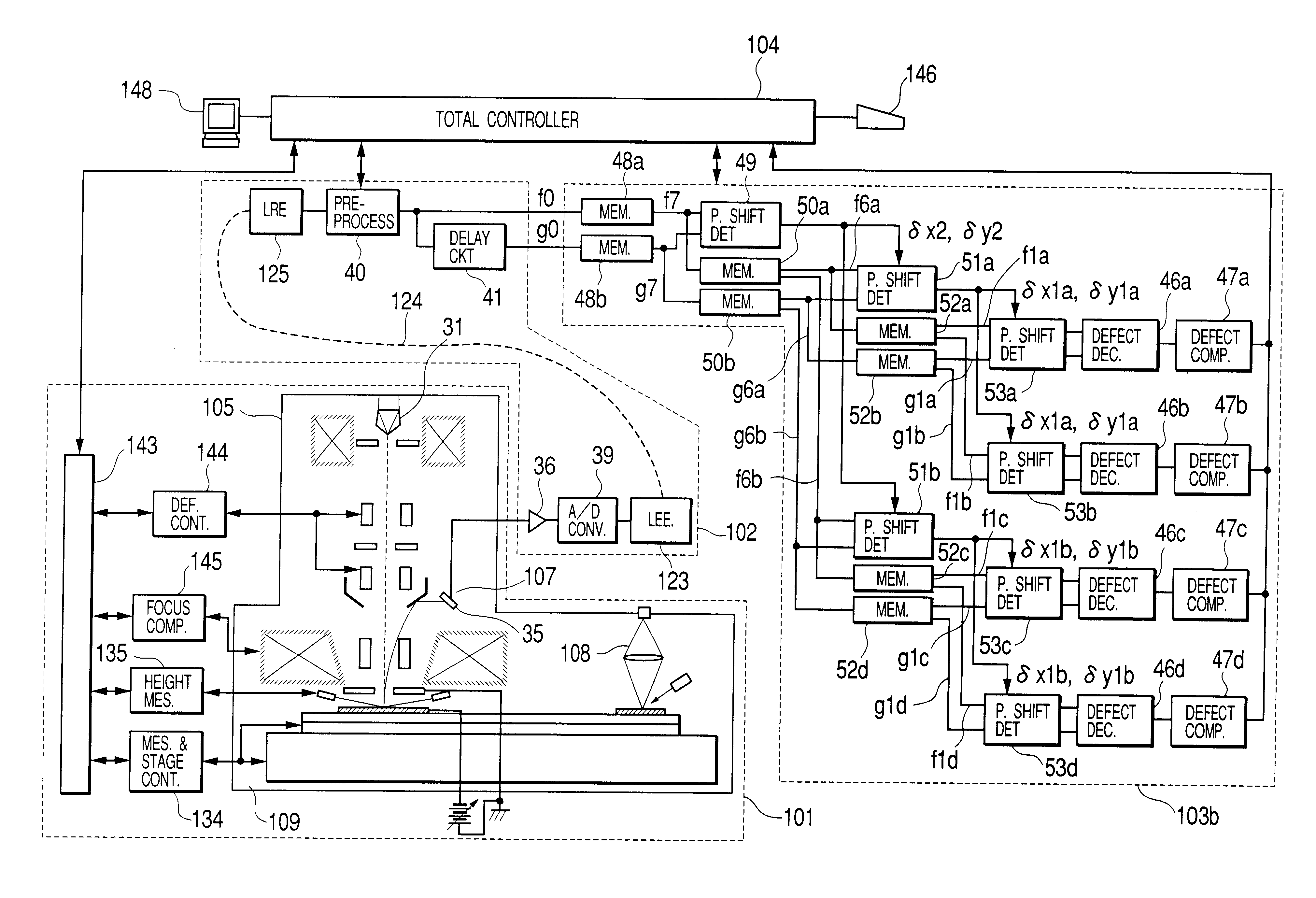
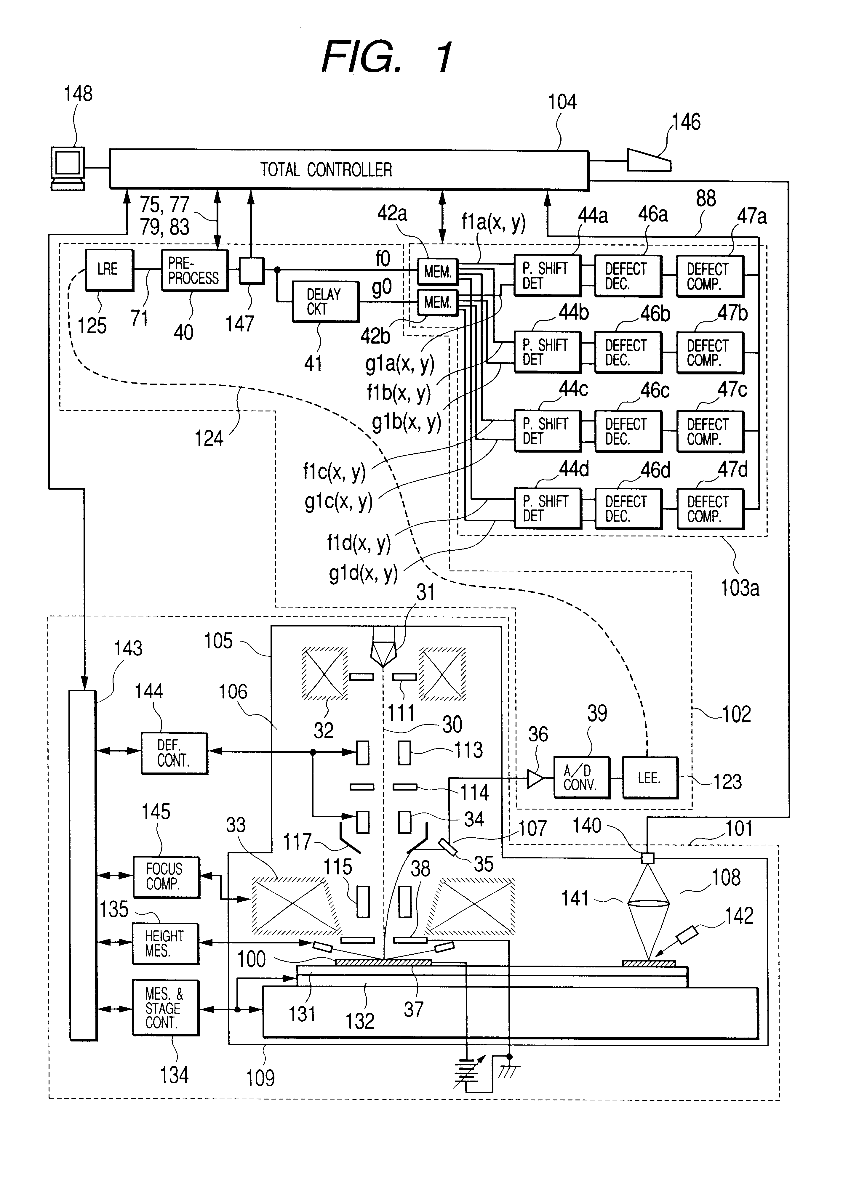
the pattern inspecting method and the apparatus thereof according to the present invention is disclosed in FIG. 1. Here, an object of inspection (i.e., test object to be inspected) 100 such as a semiconductor wafer is scanned with use of an electron gun 30, and electrons generated from the test object 100 by irradiation of the electrons are detected, thereby obtaining an image of electron beams relating a portion to be scanned depending upon changes in the intensity thereof, so as to conduct the pattern inspection with use of the electron beam image.

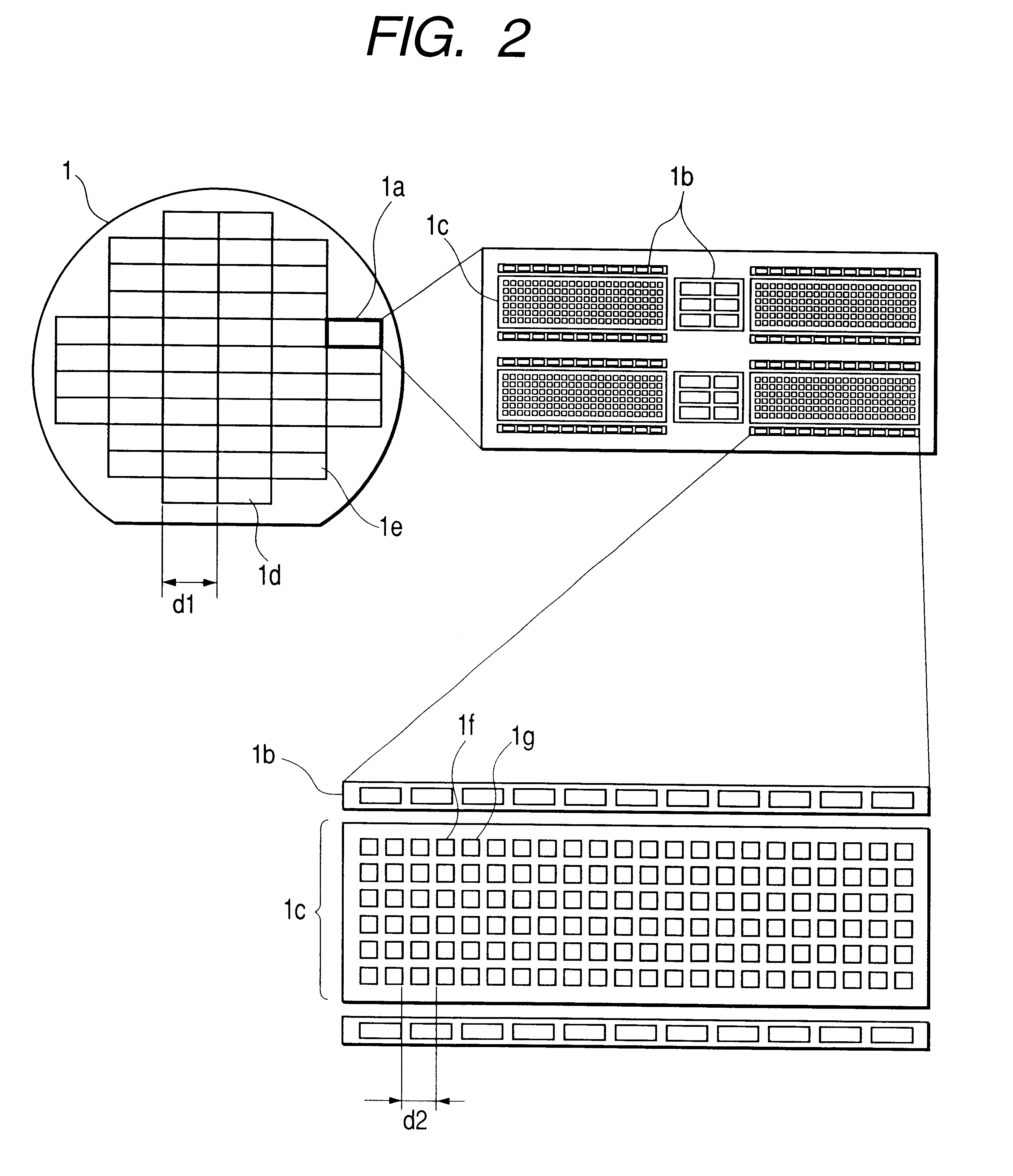
As the test object 100, it includes the semiconductor wafer 1 which is shown in FIG. 2, for example. On the semiconductor wafer 1 are formed and aligned a large number of chips 1a, each of which comes to be a same product finally. Pattern layout inside of the chip 1a comprises, as shown in an enlarged view of the same figure, memory mat portions 1c in each of which memory cells are aligned at a same pitch two-dimensionally, regularly, an...

second embodiment

The second embodiment is also same to the first embodiment described previously, as far as the image is divided finely into such the size, so as to perform the decision on the defect for each division unit, so that said the dynamic deformation or distortion can be neglected therefrom, as is shown in FIG. 7, for dealing with the dynamic deformation due to the change in the magnetic field caused by the pattern distribution of the test object 100 and / or the vibration of the stages 131 and 132, etc. The difference to the first embodiment lies in that the image is divided into such the negligible size gradually, but not from the beginning. For convenience in explanation, the first embodiment is called as "a non-stepwise division method" while the second embodiment as "a stepwise division method".

Fist of all, a concept of the stepwise division method will explained by referring to FIG. 26.

In the stepwise division method, the image is divided gradually and finally into the size being same ...


PUM


Abstract

For purpose of providing a defect inspecting method and an apparatus thereof and a defect inspecting method on basis of electron beam image and an apparatus thereof, reducing possibility of bringing erroneous or false reports due to the test objection side and the inspecting apparatus side, being caused by discrepancies, such as the minute difference in pattern shapes, the difference in gradation values, the distortion or deformation of the patterns, the position shift, thereby enabling the detection of the defects or the defective candidates in more details, wherein an image which is small in distortion by controlling the electron beam scanning is detected and divided into a size so as to be able to neglect therefrom, and then position shift detection and defect decision are carried out in an accuracy less or finer than pixel for each division unit. In the defect decision, a desired tolerance can be set up depending upon changes in gradation values and the position shift.

Description

1. Field of the InventionThe present invention relates to a pattern inspecting method and an apparatus thereof, and a pattern inspecting method on a basis of an electron beam pictures or images and an apparatus thereof, with which a picture, displaying physical properties of an object such as a semiconductor wafer, TFT, a photo mask and so on, is obtained by use of an electron beam, a light or the like, and the obtained picture is compared with a picture which is obtained separately therefrom, thereby detecting defects or quasi-defects (or defective candidates), in particular the fine or minute ones thereof.In a conventional art 1, as is described in Japanese Patent Laying-Open No. Sho 57-196377 (1982), there is already know a testing or an inspection, wherein a pattern including a repetitive pattern, being formed on an object to be tested or inspected such as a semiconductor wafer, is detected to be memorized, and the detected pattern is fitted or aligned with to a pattern which is...

Claims


Application Information

Patent Timeline
IPC IPC(8): G06T7/00G01B11/30G01R31/302G06T1/00G06T5/00H01J37/22H01J37/28H01L21/027H01L21/66
CPCG06T5/006G06T7/001H01J37/226H01J37/28G06T2207/10061G06T2207/30148H01J2237/2448H01J2237/24592H01J2237/2482H01J2237/2806H01J2237/2817
Inventor SHISHIDO, CHIETAKAGI, YUJIMAEDA, SHUJININOMIYA, TAKANORIHIROI, TAKASHIWATANABE, MASAHIRODOI, HIDEAKI
Owner HITACHI LTD
Why Eureka
Try Eureka