Strain-relieved tunable dielectric thin films

a dielectric thin film, strain-relieving technology, applied in waveguide devices, natural mineral layered products, vacuum evaporation coatings, etc., can solve the problems of high power needed to operate current ferrite-based devices, tunable microwave devices based, and current semiconductor-based devices that exhibit substantial losses at frequencies over 2 ghz

Inactive Publication Date: 2003-09-09
NXP USA INC
View PDF21 Cites 24 Cited by
  • Summary
  • Abstract
  • Description
  • Claims
  • Application Information

AI Technical Summary

Benefits of technology

In accordance with an embodiment of the present invention, the thin BST buffer layer relieves the film strain caused by film / substrate mismatches, i.e., lattice and thermal expansion mismatches between the film and substrate during the film deposition process and post-annealing process. The strain-relieved and defect-reduced tunable dielectric thin film according to the invention provides higher dielectric quality factors at high frequencies (.gtoreq.2 GHz) than currently existing prior art semiconductor materials as well as other prior art ferroelectric materials. Thus, the present invention provides a tunable dielectric thin film for tunable microwave applications, and a method of formation thereof, which relieves film strain having a significant effect on both microstructure and microwave dielectric properties of the film.
Another aspect of the present invention is to provide a method of making a thin film dielectric material. The method comprises the steps of depositing a thin dielectric buffer layer on a low dielectric loss substrate at a first temperature, and depositing a layer of dielectric thin film on the dielectric buffer layer at a second temperature. The deposited layers may be annealed to reduce crystalline defects and to grow crystalline grains.

Problems solved by technology

This results from disadvantages associated with currently available tunable microwave devices based on PIN diodes and ferrites.
Current semiconductor-based devices exhibit substantial losses at frequencies over 2 GHz, and high power is needed to operate current ferrite-based devices.
Although attempts have been made at developing tunable dielectric thin films having low dielectric losses, and improvements have been made at low frequencies (.ltoreq.1 MHz), prior art methods are not conducive to the use of these films in tunable applications at high frequencies (i.e., .gtoreq.2 GHz).
Tunable dielectric materials having significantly increased Q values at low frequencies (.ltoreq.1 MHz) developed in the prior art are not commercially viable because currently available semiconductor materials have much better performance at those frequencies than the conventionally developed dielectric materials.
As a dielectric film is strained during film deposition processes and post-annealing processes due to thermal expansion mismatch between the film and substrate, conventional films do not have desirable dielectric properties exhibiting both high dielectric Q and high dielectric tuning because of the film strain, even though structural defects are significantly reduced and crystalline grains are largely grown in the film during the post-annealing.
Therefore, as long as a substantial strain-induced structural distortion exists in the film, the microwave dielectric properties of the film cannot exhibit both large dielectric tuning and high dielectric Q at the same time.

Method used


Image

  • Strain-relieved tunable dielectric thin films
  • Strain-relieved tunable dielectric thin films
  • Strain-relieved tunable dielectric thin films

Examples


example 1

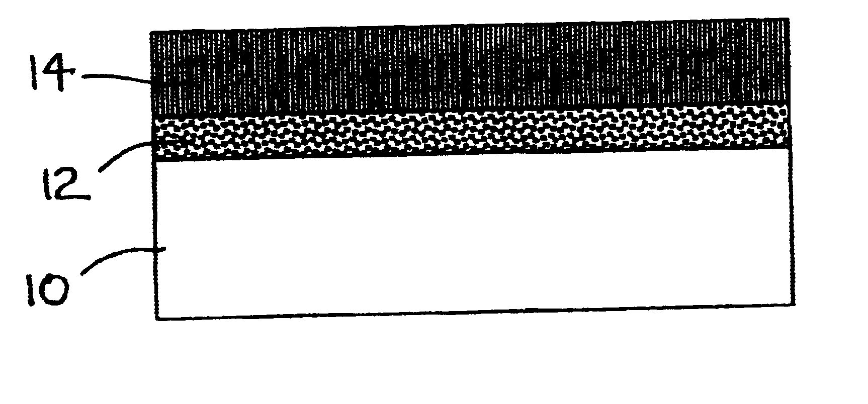
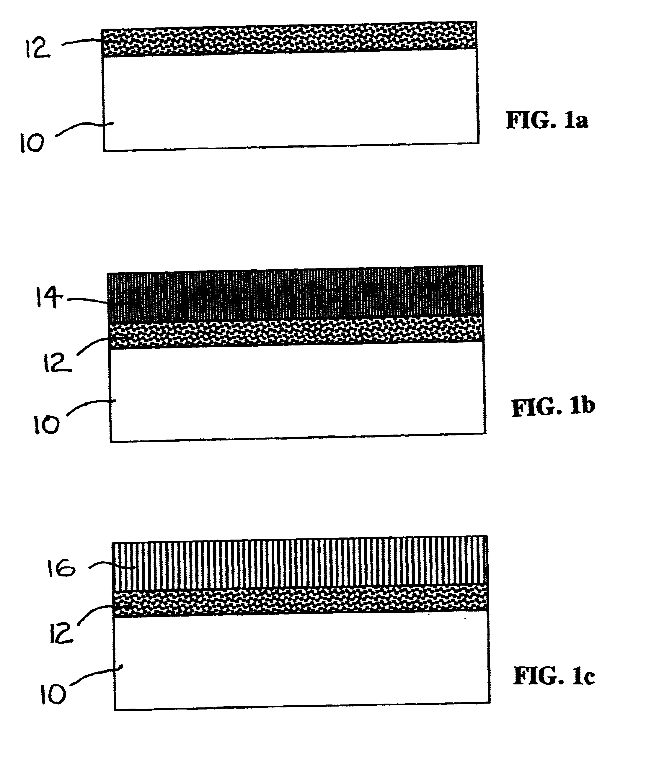
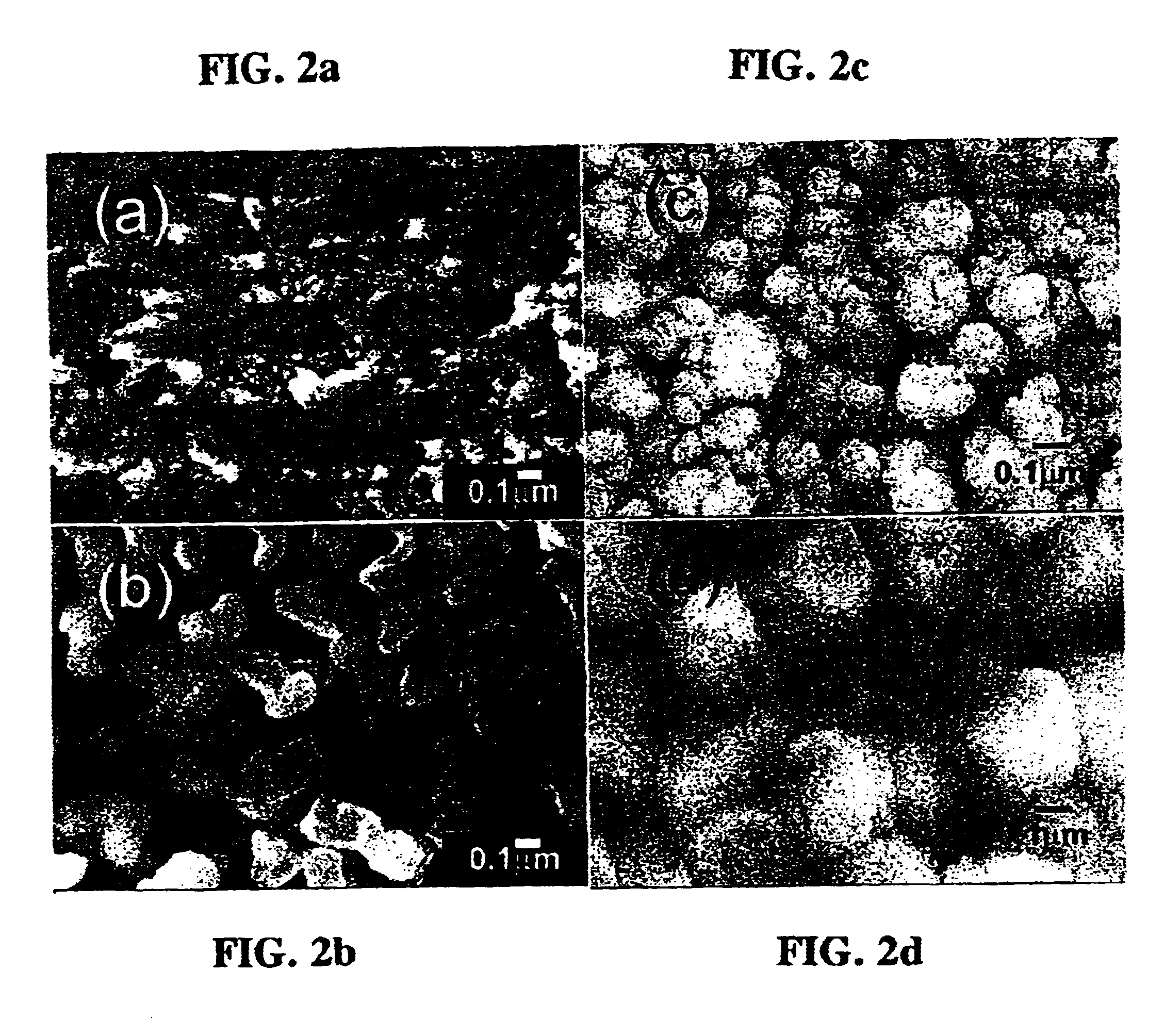
A number of tunable dielectric thin films were fabricated to demonstrate the superior dielectric properties at microwave frequencies of the film according to the present invention over currently existing prior art semiconductor materials as well as other prior art ferroelectric materials. First, a thin (<0.1 .mu.m thick) amorphous BST (x=0.4) buffer layer was deposited on (001) MgO low dielectric loss, single crystal substrate at room temperature in an oxygen background pressure of 200 mTorr by pulsed laser deposition (PLD). The output of a short-pulsed (30 ns full width at half maximum) eximer laser operating with KrF (.lambda.=248 nm) at 1 Hz was focused to a spot size of .about.0.1 cm.sup.2 and an energy density of 1.9 J / cm.sup.2 onto a single-phase BST (x=0.4) target. The vaporized material was deposited onto (001) MgO substrate approximately 5 cm away from the target. The microstructure of BST buffer layer can be modified into any phase between an almost amorphous phase and a r...

example 2

Characterization of small signal microwave properties of a planar varactor containing a strain-relieved and defect-reduced BST (x=0.4) thin film with a BST (x=0.4) buffer layer according to the present invention was made at room temperature using a gap-coupled half-wavelength (.lambda. / 2) stripline resonator connected to an HP 8510C network analyzer.

FIG. 5a illustrates a planar varactor 18 based on a strained but defect-reduced epitaxial BST (x=0.4) film 20 deposited directly on a (001) MgO substrate 10 without a BST (x=0.4) buffer layer, and then annealed in flowing oxygen at 1,000.degree. C. for 6 hours. FIG. 5b illustrates a planar varactor 24 based on a strain-relieved and defect-reduced randomly oriented crystalline BST (x=0.4) film 16 deposited on a (001) MgO substrate 10 with a BST (x=0.4) buffer layer 12 in accordance with the present invention, and then annealed in flowing oxygen at 1,000.degree. C. for 6 hours. For both types of varactor shown in FIGS. 5a and 5b, single-ga...


PUM

PropertyMeasurementUnit
thicknessaaaaaaaaaa
thicknessaaaaaaaaaa
thicknessaaaaaaaaaa

Abstract

Tunable dielectric thin films are provided which possess low dielectric losses at microwave frequencies relative to conventional dielectric thin films. The thin films include a low dielectric loss substrate, a buffer layer, and a crystalline dielectric film. Barium strontium titanate may be used as the buffer layer and the crystalline dielectric film. The buffer layer provides strain relief during annealing operations.

Description

The present invention relates to tunable dielectric thin films, and more particularly relates to strain-relieved and defect-reduced tunable dielectric thin films which significantly reduce dielectric loss at microwave frequencies.BACKGROUND INFORMATIONConsiderations in the development of tunable microwave devices based on ferroelectric materials are the dielectric constant, tunability and the dielectric quality factor (Q=1 / tan .delta.) of the materials. The DC electric field dependent dielectric constant of ferroelectric thin films, such as Ba.sub.1-x Sr.sub.X TiO.sub.3 (BST, 0.ltoreq.x.ltoreq.1), is currently being used to develop low loss tunable microwave devices, such as voltage-controlled oscillators, tunable filters and phase shifters. This results from disadvantages associated with currently available tunable microwave devices based on PIN diodes and ferrites. Current semiconductor-based devices exhibit substantial losses at frequencies over 2 GHz, and high power is needed to...

Claims


Application Information

Patent Timeline
Patent Type & Authority Patents(United States)
IPC IPC(8): C23C14/08H01P1/18H01P7/08
CPCC23C14/088H01P1/181H01P7/082H01P7/084H01P7/088
Inventor CHANG, WONTAE
Owner NXP USA INC
Why Eureka
Try Eureka