

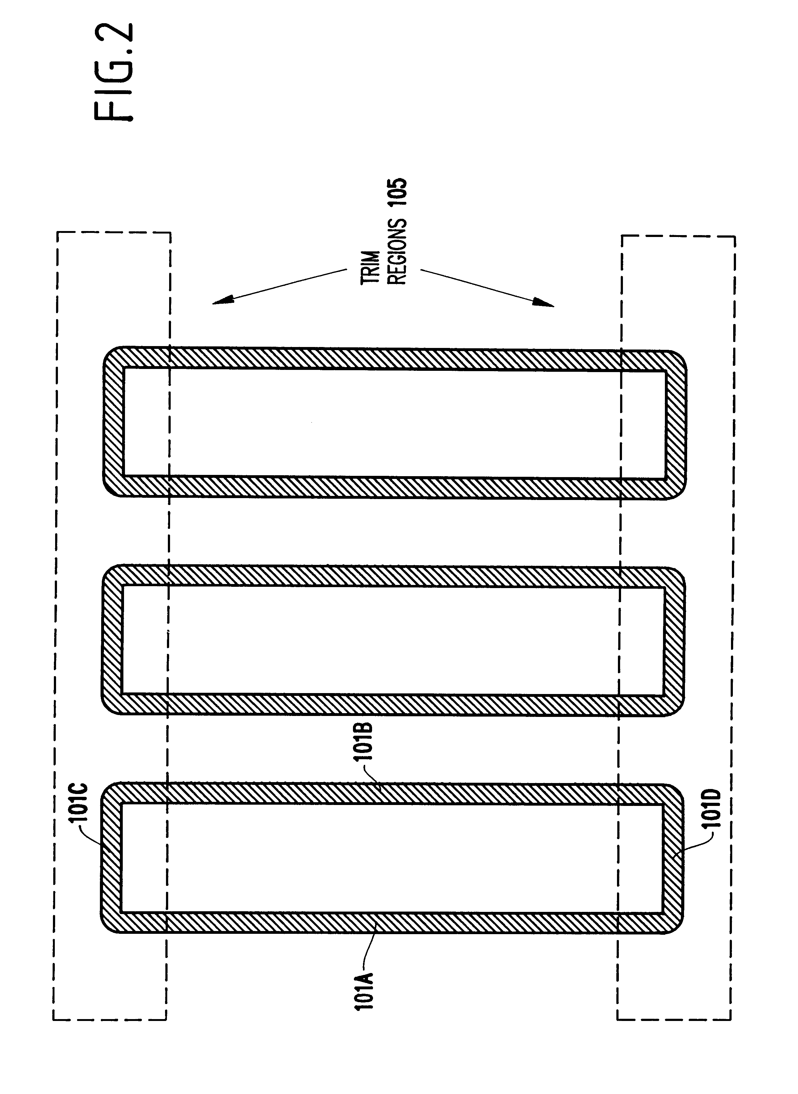
Self-trimming method on looped patterns
- Summary
- Abstract
- Description
- Claims
- Application Information
AI Technical Summary
Benefits of technology
Problems solved by technology
Method used
Image

Examples
embodiment
PREFERRED EMBODIMENT
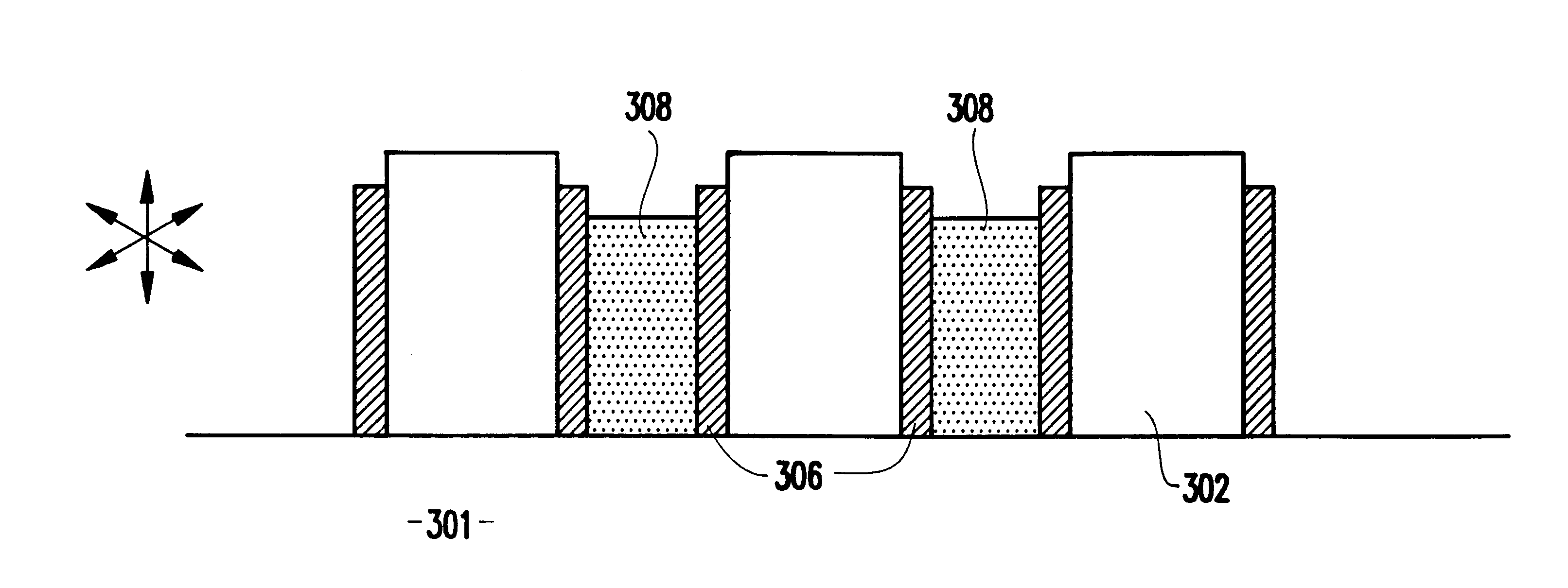
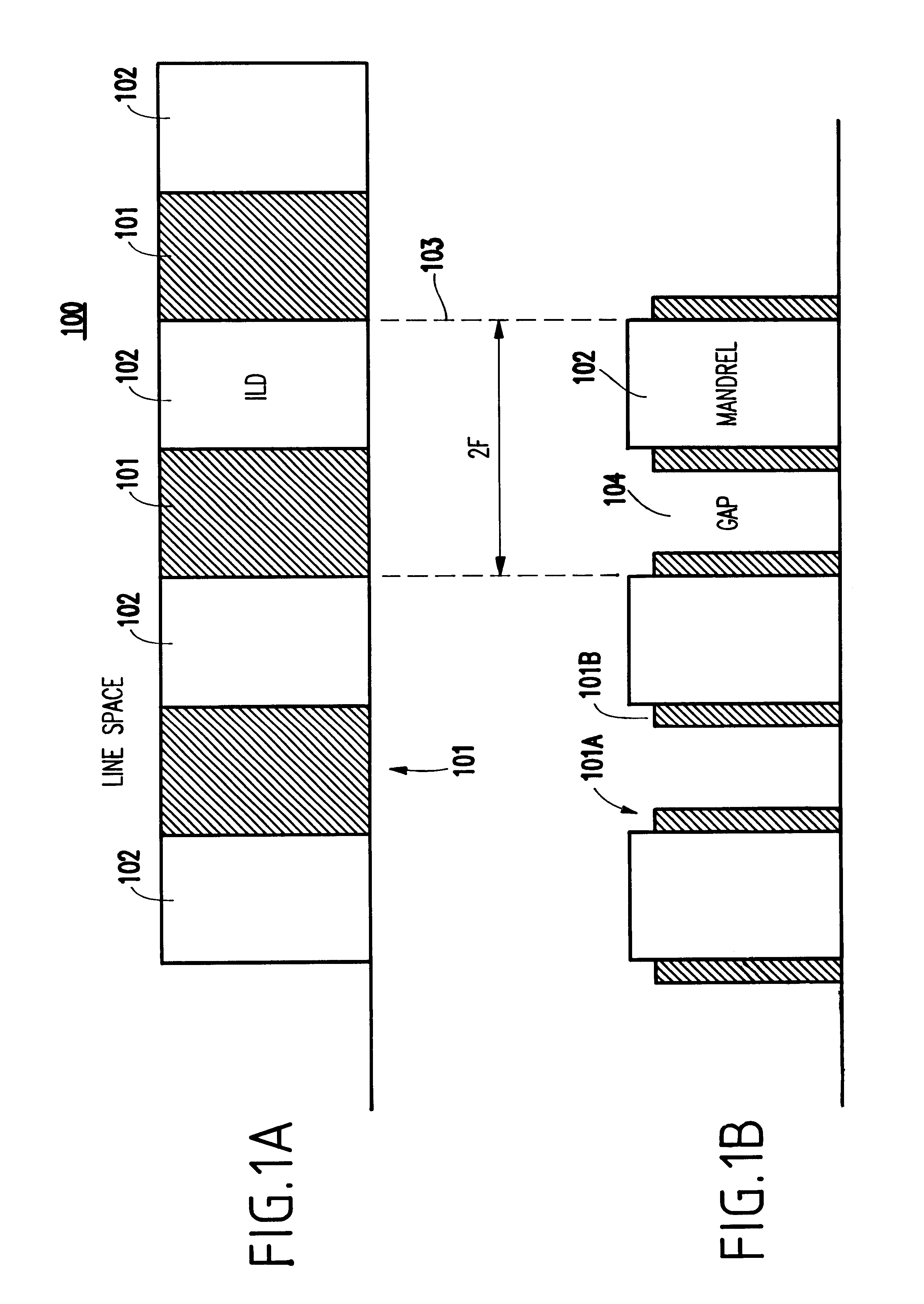
A cross-sectional view of a conventional line / space pattern 100 formed of, for example, an electrically conductive material 101, and an electrically insulating material 102, is shown in FIG. 1A. It is noted that, in the invention, the conducting material and insulating material could be changed (e.g., an analog arrangement could be produced to what is shown in FIGS. 1A-9) to the other. The conducting material 101 may be a metal such as Al, W, TiN, Cu, TiW, Ta, polysilicon, or some combination of electrically conductive materials. The insulating materials 102 between the conductors 101 may be a dielectric such as silicon dioxide, CVD oxide, TEOS, doped glass, or polymers.
The line / space pattern 100 of conductors may be formed using conventional photolithography technique such as imaging of a photoresist mask to a metal layer followed by metal etching such as reactive ion etching (RIE), and deposition of a interlevel dielectric (ILD) such as silicon dioxide. The lin...
PUM
 Abstract
Description
Claims
Application Information