Solder reflow with microwave energy

a microwave energy and soldering technology, applied in the field of flip chip packaging, can solve the problems of thermal mismatch, delamination and cracks which tend to propagate, and the performance and reliability of chips are becoming limited

Inactive Publication Date: 2003-11-11
INTEL CORP
View PDF17 Cites 54 Cited by
  • Summary
  • Abstract
  • Description
  • Claims
  • Application Information

AI Technical Summary

Problems solved by technology

However, as transistor sizes continue to shrink, chip performance and chip reliability are becoming limited by the chip-to-package interconnections.
However, all components on the die and the substrate are heated so damage may result, especially during cool down, from the large stresses that arise at interfaces between different materials.
Such thermal mismatch occurs because the Coefficient of Thermal Expansion (CTE) of the substrate may be about ten times larger than the CTE of the chip.
The large stresses may lead to delamination and cracks which tend to propagate when the chip is thermally loaded, especially under conditions of high humidity.

Method used


Image

  • Solder reflow with microwave energy
  • Solder reflow with microwave energy
  • Solder reflow with microwave energy

Examples


Embodiment Construction

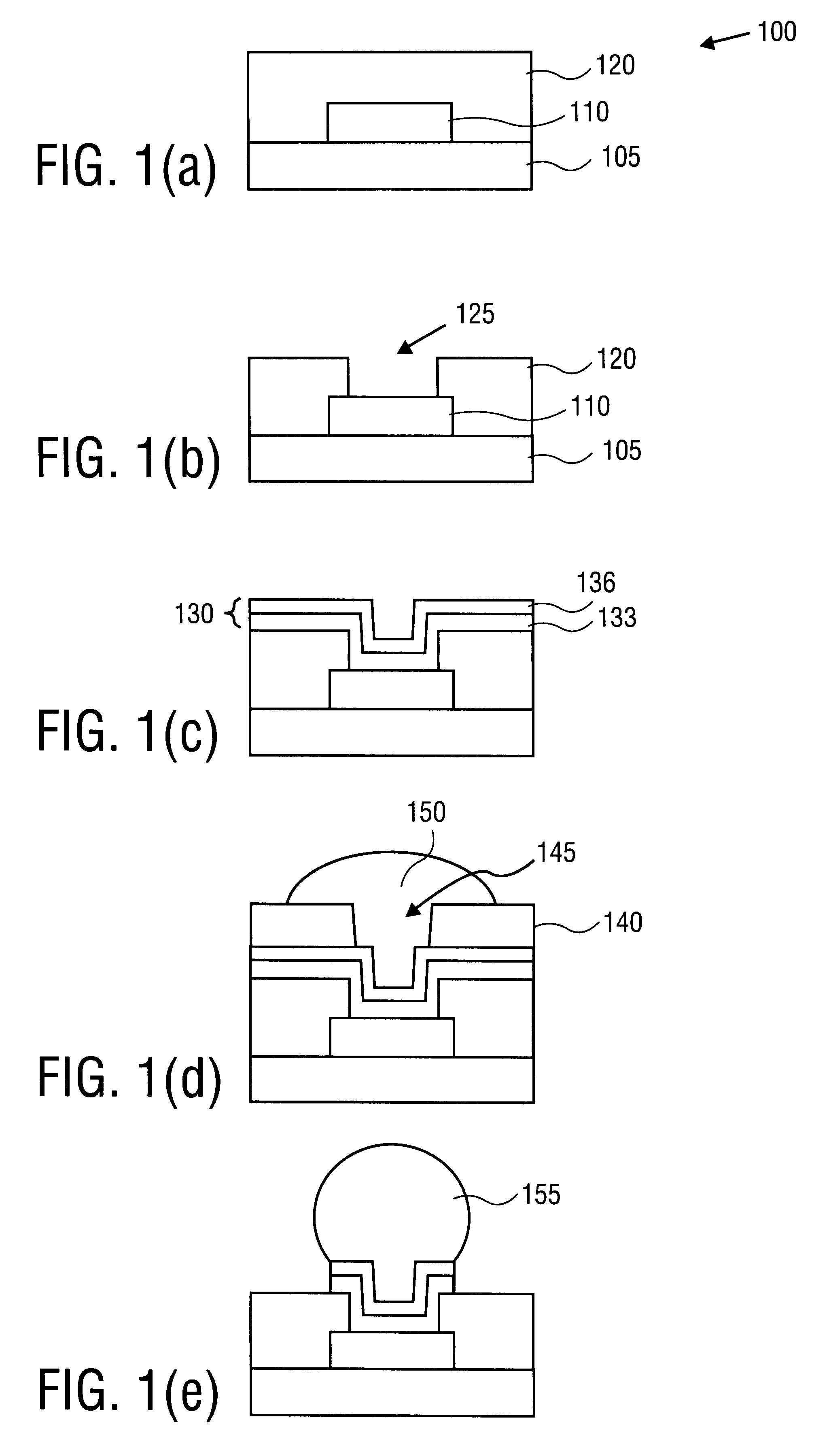
In the following description, numerous particular details, such as specific materials, dimensions, and processes, are set forth in order to provide a thorough understanding of the present invention. However, one skilled in the art will realize that the invention may be practiced without these particular details. In other instances, well-known semiconductor equipment and processes have not been described in particular detail so as to avoid obscuring the present invention.

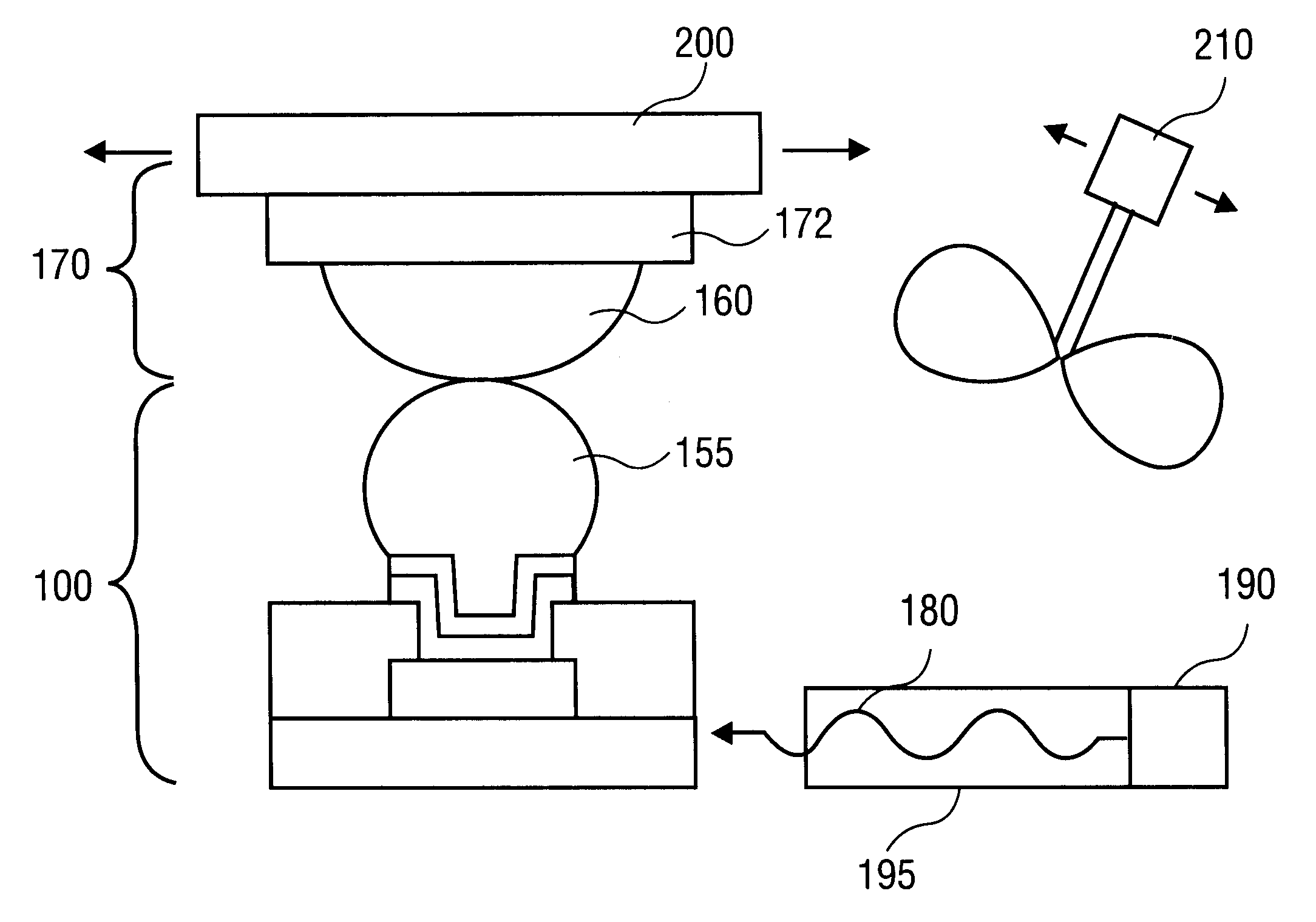
The present invention comprises a mechanical joint between a substrate and a die and a method of using microwave energy to form the mechanical joint. Microwave energy may be used to selectively reflow solder on the substrate to form the mechanical joint with input / output (I / O) connections at the surface of the die or flip chip. The mechanical joint in Surface Mount Technology (SMT) allows an electrical connection for power, ground, or signal in and out of the die.

In one embodiment, the substrate may be an interposer ...


PUM

PropertyMeasurementUnit
temperatureaaaaaaaaaa
thicknessaaaaaaaaaa
thicknessaaaaaaaaaa

Abstract

The present invention includes a mechanical joint between a die and a substrate that is reflowed by microwave energy and a method of forming such a mechanical joint by printing a solder over a substrate, placing the solder in contact with a bump over a die, reflowing the solder with microwave energy, and forming a mechanical joint from the solder and the bump.

Description

1. Field of the InventionThe present invention relates to the field of semiconductor integrated circuit (IC) manufacturing, and more specifically, to a method of packaging flip chips.2. Discussion of Related ArtChip-to-package interconnections have traditionally involved wirebonding. Wirebonding is the use of very fine metal wires to join the contacts at the top surface of the chip with the corresponding contacts at the top surface of the substrate. However, as transistor sizes continue to shrink, chip performance and chip reliability are becoming limited by the chip-to-package interconnections. Consequently, wirebonding is being superseded by solder bumping.Solder bumping has many advantages over wirebonding. First, bumps may be placed anywhere over the chip so the input / output (I / O) density is significantly increased. Second, the bumps reduce the length of the interconnections so chip performance is greatly enhanced. Third, eliminating the edge-connections associated with wirebond...

Claims


Application Information

Patent Timeline
Patent Type & Authority Patents(United States)
IPC IPC(8): B23K1/008H05K3/34
CPCB23K1/008H05K3/3494H05K3/3436B23K2201/40B23K2101/40H01L24/05H01L24/11H01L24/81H01L2224/05001H01L2224/05022H01L2224/05027H01L2224/0508H01L2224/05572H01L2224/1134H01L2924/00011H01L2924/01322H01L2924/12042H01L2924/14H01L2924/00H01L2924/00014H01L2224/81805
Inventor RATIFICAR, GLENNGONZALEZ, CARLOSWANG, LEJUN
Owner INTEL CORP
Why Eureka
Try Eureka