Check patentability & draft patents in minutes with Patsnap Eureka AI!

Magnetic snapback sensor circuit and electrostatic discharge circuit using same

a technology of magnetic snapback and sensor circuit, applied in emergency protective circuit arrangements, instruments, etc., can solve the problems of timer not working as intended, transistor gate oxide and oxide-silicon interface damag

Inactive Publication Date: 2003-11-18
ANALOG DEVICES INC
View PDF6 Cites 9 Cited by
  • Summary
  • Abstract
  • Description
  • Claims
  • Application Information

AI Technical Summary

Problems solved by technology

One problem with this approach is that during the high current exposure of the MOS transistor during the ESD event, the transistor gate oxide and oxide-silicon interface can be damaged by hot electrons emanated from the adjacent avalanching drain to backgate junction diode.
A problem with the timer circuit approach above is that for low voltage ESD events, the time between timer activation and the ESD-induced activation voltage reaching a high enough threshold causes the timer to shut off (lower the voltage) on the MOS gate, which reintroduces the snapback high voltage the transistor is meant to shut off.
Thus if the voltage took too long to reach a predetermined trigger level the timer would not operate as intended.

Method used


Image

  • Magnetic snapback sensor circuit and electrostatic discharge circuit using same
  • Magnetic snapback sensor circuit and electrostatic discharge circuit using same
  • Magnetic snapback sensor circuit and electrostatic discharge circuit using same

Examples


Embodiment Construction

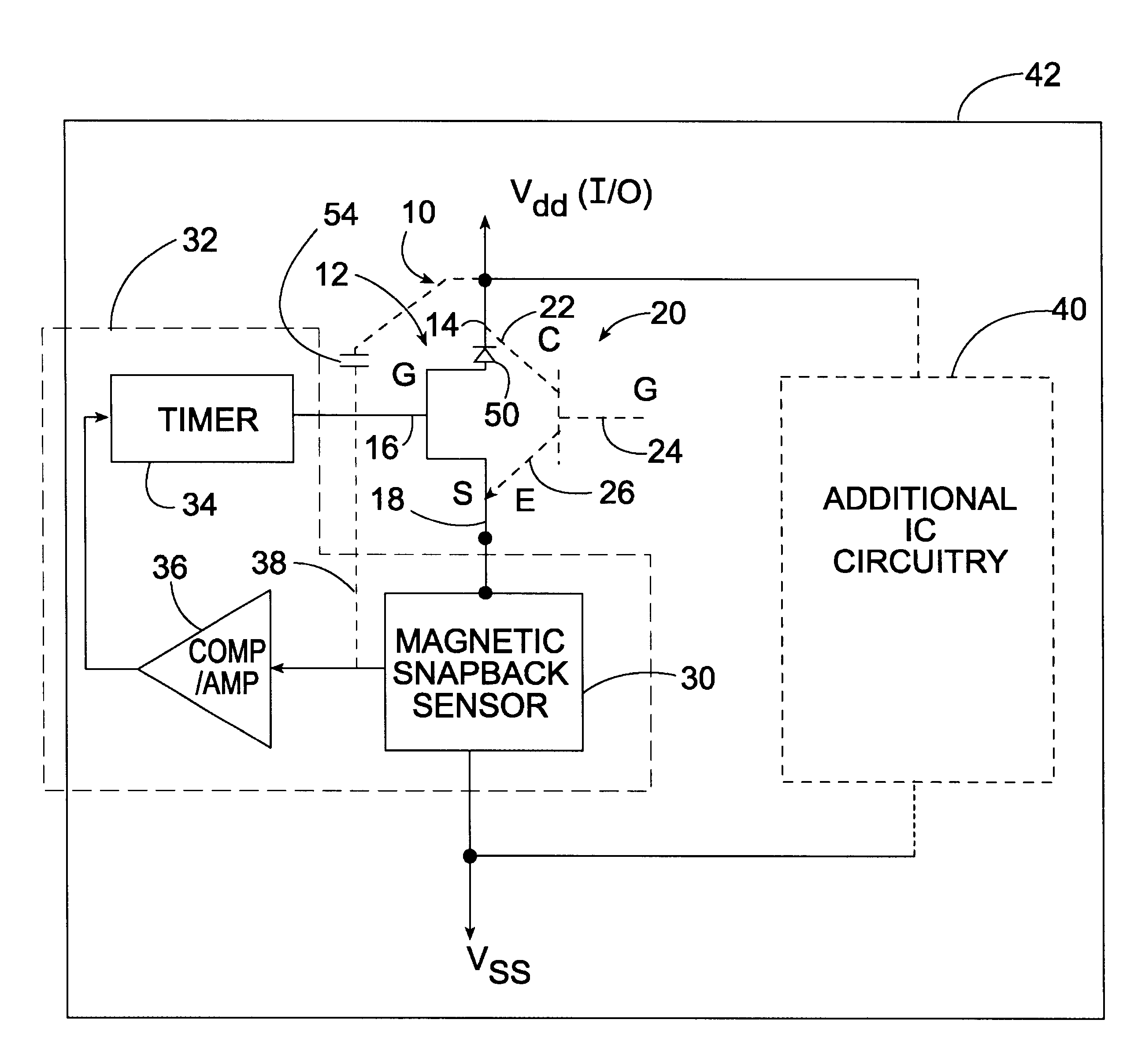
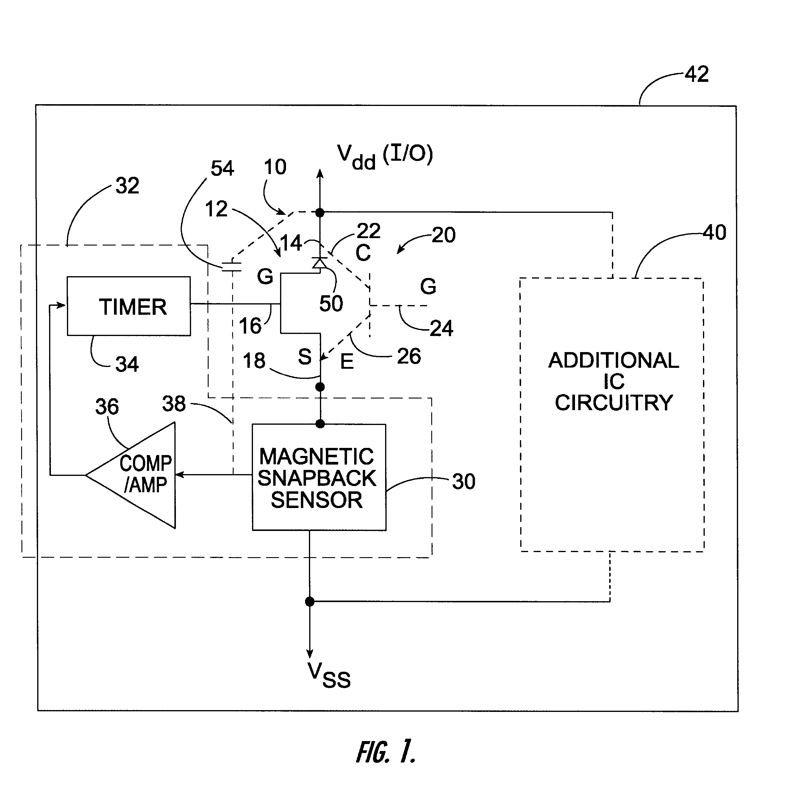
There is shown in FIG. 1 a snapback circuit 10 including an MOS transistor 12 having a drain 14, gate 16, and source 18. Associated with it is the inherent parasitic npn-type bipolar transistor 20 including collector 22, backgate base 24, and emitter 26. Snapback circuit 10 is connected in series with magnetic snapback sensor 30 between the power supply terminals Vdd and Vss, or alternatively between the I / O terminal in place of Vdd and terminal Vss. Magnetic snapback sensor 30 forms a part of a magnetic snapback sensor circuit 32 which may also include a timer 34 and a comparator or amplifier 36. The output for the magnetic snapback sensor 30 may be used in an adaptation of timer circuit 34 such as taught by U.S. Pat. No. 5,940,258. If the output signal voltage from magnetic snapback sensor 30 is not of a sufficient level to bias a MOS transistor gate 12 above threshold comparator or amplifier 36 may be used to boost the signal either to timer 34 or directly to gate 16. Snapback ci...


PUM


Abstract

A magnetic snapback sensor circuit for sensing current transients imposed on the snapback circuit including a current conductor loop; a conductor carrying current from a snapback circuit subject to current transients and intersecting with the conductor loop for magnetically generating a current in the loop; and a current detector circuit for generating an output responsive to the current flowing in the loop induced by a current transient.

Description

This invention relates to a magnetic snapback sensor circuit, and to such a magnetic snapback sensor circuit useful in an electrostatic discharge (ESD) circuit.BACKGROUND OF INVENTIONSnapback circuits employ the inherent parasitic bipolar transistor associated with each MOS transistor to accommodate increased current flow through such bipolar transistor to lower the maximum voltage at the MOS drain electrode in response to an electrostatic discharge. The original publication describing the snapback operation is "Snap-Back; A Stable Regenerative Breakdown Mode of MOS Devices," A. Ochoa, Jr., F. W. Sexton, T. F. Wrobel, G. L. Hash and R. J. Sokel, IEEE Transactions on Nuclear Science, Vol. NS-30, No. 6, pp. 4127-4130, December 1983. Electrostatic discharge generated by, for example, a person walking on a rug can introduce transient high voltage current flow of up to 2-3 amps for up to 150 nanoseconds, enough to damage or destroy integrated circuit components. One shortcoming to such s...

Claims


Application Information

Patent Timeline
Patent Type & Authority Patents(United States)
IPC IPC(8): G01R31/28G01R33/06G01R33/07H02H9/00H01L27/02
CPCH01L27/0266
Inventor RIGHTER, ALAN W.
Owner ANALOG DEVICES INC
Features
  • R&D
  • Intellectual Property
  • Life Sciences
  • Materials
  • Tech Scout
  • Unparalleled Data Quality
  • Higher Quality Content
  • 60% Fewer Hallucinations
Learn More