Supercharge Your Innovation With Domain-Expert AI Agents!

On chip programmable data pattern generator for semiconductor memories

a data pattern generator and semiconductor technology, applied in the field of semiconductor memories, can solve the problems of increasing the difficulty and cost of testing memories, rapid growth of circuit complexity, and the introduction of a new dimension of testing complexity in the development of high density memories

Inactive Publication Date: 2003-11-18
POLARIS INNOVATIONS
View PDF13 Cites 8 Cited by
  • Summary
  • Abstract
  • Description
  • Claims
  • Application Information

AI Technical Summary

Problems solved by technology

The rapid growth in circuit complexity has increased the difficulty and cost of testing memories.
Development of high density memories introduces a new dimension in testing complexity.
For example, higher speed synchronous DRAMs need includes more complex and more time consuming pattern testing.
It is typically expensive to add additional testers at to maintain the throughput needed for more complex high-speed memory devices.
Another issue concerning the testing of both the current and future generations of high density memories involves chip frequencies relative to the speed and accuracy of the testers.
It is becoming more difficult to find high-speed test systems that can keep up with the chips being tested.
At the same time, the test equipment is getting more complex.
Further, maintaining costs at a reasonable level and performing the tests in a reasonable time frame are also an issue for manufactures and testers.
Due to the address information and the density of memory cells difficulties arise with respect to testing.
Testing costs are presently a major contributor to overall manufacturing costs of memory chips.
The number of chips tested in parallel is usually limited by the number of input / output (I / O) channels a memory tester can handle.

Method used


Image

  • On chip programmable data pattern generator for semiconductor memories
  • On chip programmable data pattern generator for semiconductor memories
  • On chip programmable data pattern generator for semiconductor memories

Examples


Embodiment Construction

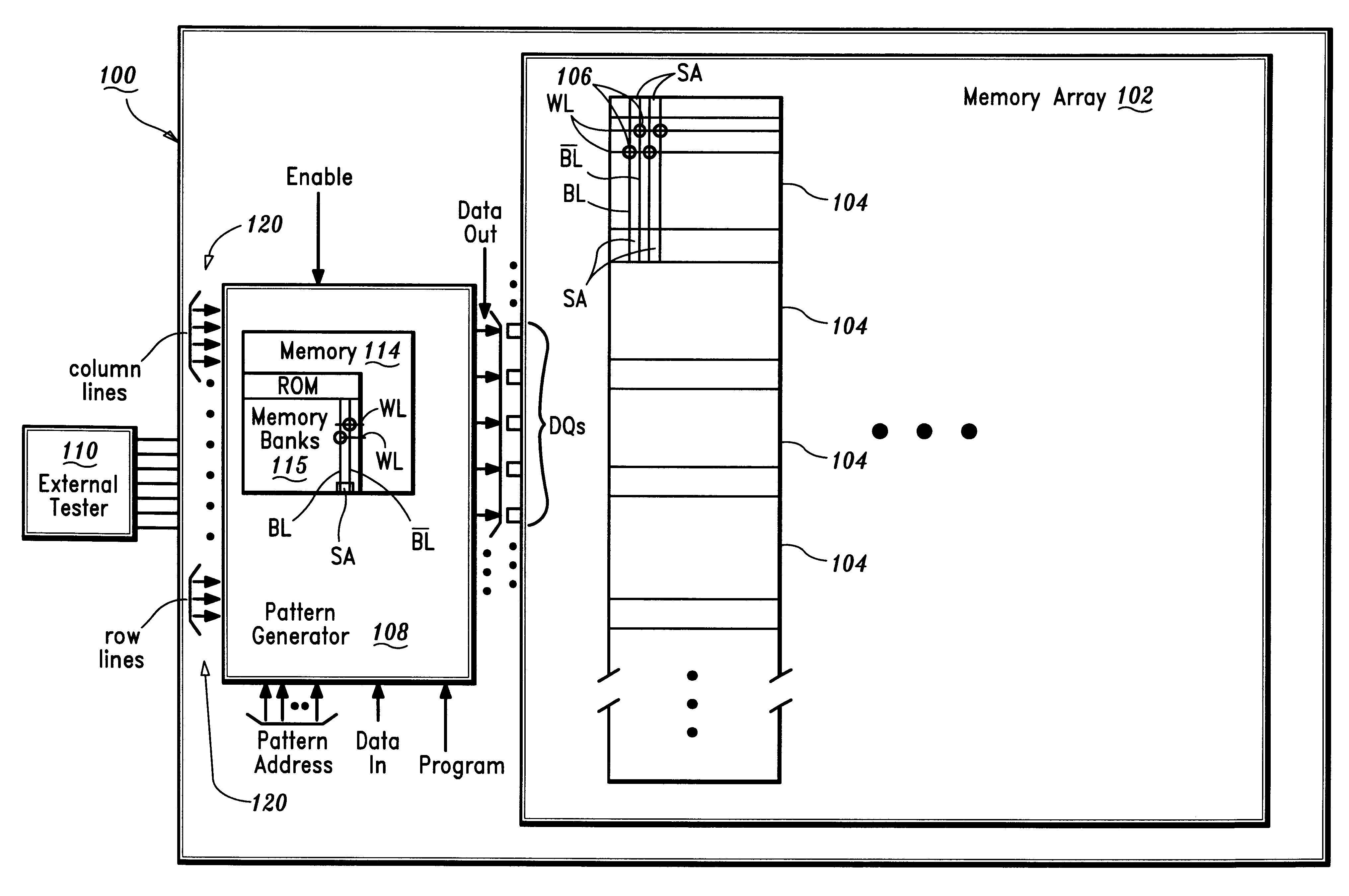
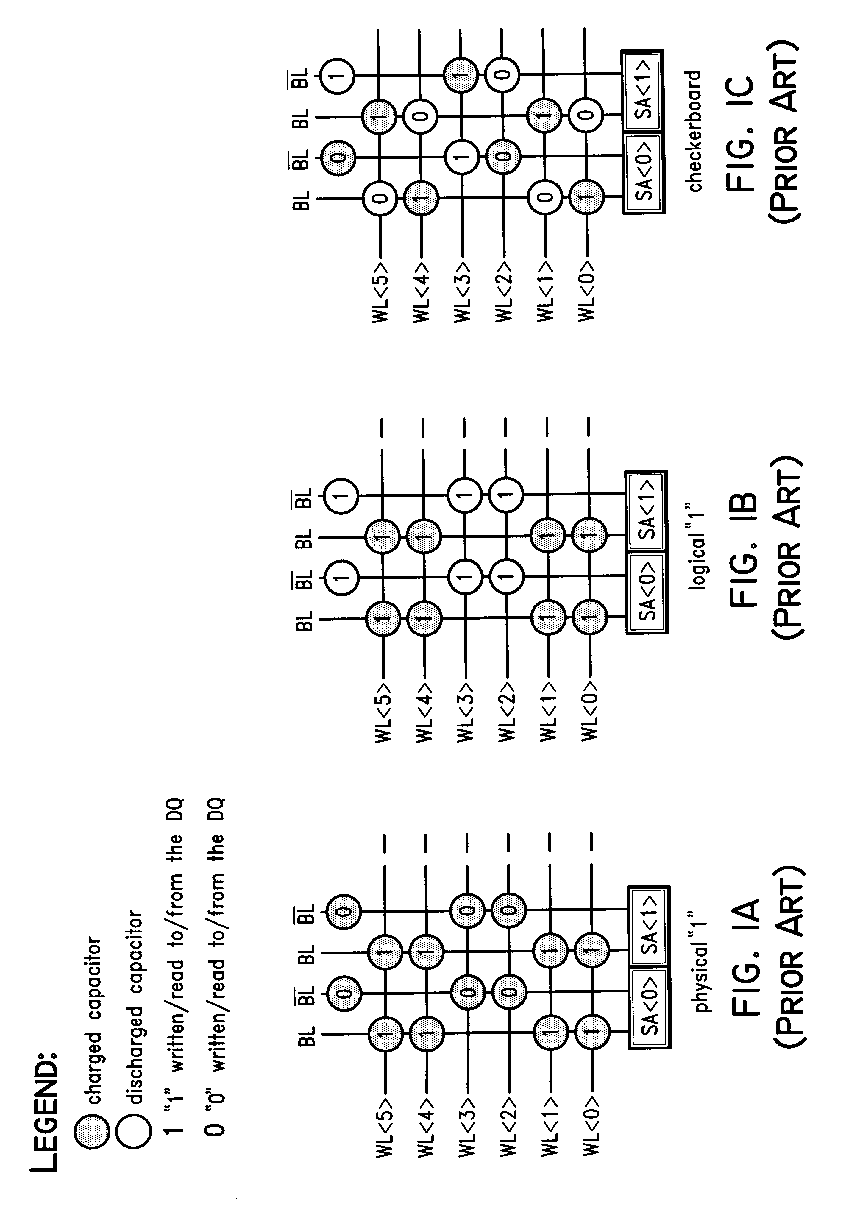
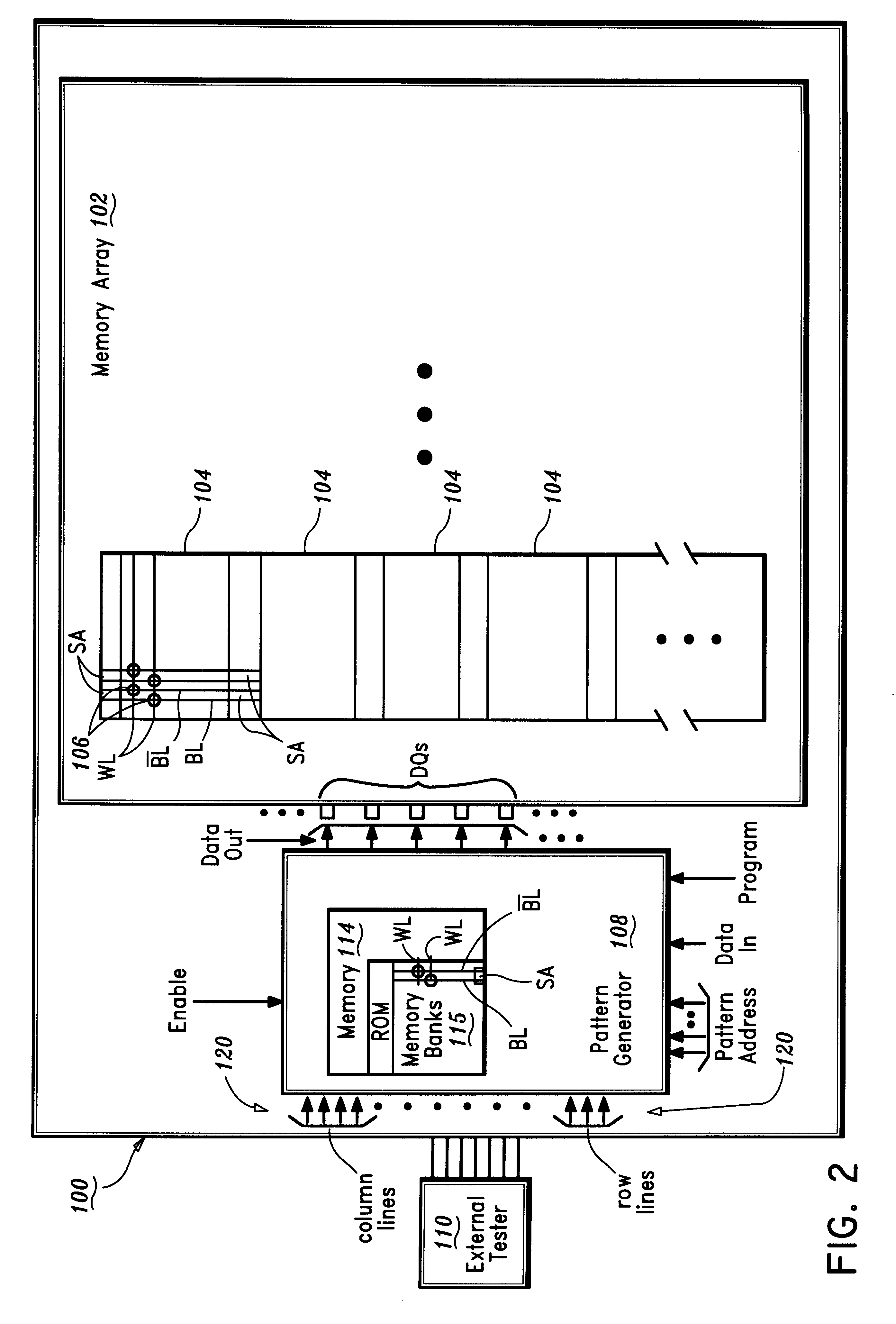
The following Example illustratively describes a pattern generator in accordance with the present invention for a 16 bit DRAM chip. For a 16 bit chip DQs 0-15 are included. For this example, memory architecture permits a pattern with 2 column bits, i.e., n=2, and 4 bits in the row direction, i.e., m=4. Also, 8 patterns are desired to be stored in the patten generator memory, then k=7 (0-7 is 8 patterns). (WLs are decoded from the row address, m) m and n are related to the smallest repeatable structure in the array in terms of topology. It is desired to write a checkerboard pattern (See FIG. 1C). The pattern generator has to provide the 0's and 1's of the pattern. Referring to FIG. 1C, in the case of activating sense amp SA , the y-address would be 0, and x-address (WL) is also 0, and a 1 is applied to the bitline BL. Now, if the x-address is changed from 0 to 1 (to WL ), a 0 is needed at the output of the pattern generator. From WL to WL 1, the same y-address is used.

For the patte...


PUM


Abstract

A semiconductor memory chip in accordance with the present invention includes a first memory array to be tested including a plurality of memory cells arranged in rows and columns, the memory cells being accessed to read and write data thereto by employing bitlines and wordlines, the data provided on input / output pins, and a pattern generator formed on the memory chip. The pattern generator further includes a programmable memory array including a plurality of memory banks, the memory banks having memory cells arranged in rows and columns, each bank being capable of storing data for a pattern to be generated for each of the input / output pins of the first memory array. An addressing circuit for accessing the data stored in the programmable memory array to address individual data to be transmitted to and from the first memory array is included.

Description

1. Technical FieldThis disclosure relates to semiconductor memories and more particularly, to an apparatus for testing memory devices using an on chip data pattern generator.2. Description of the Related ArtThe rapid growth in circuit complexity has increased the difficulty and cost of testing memories. Development of high density memories introduces a new dimension in testing complexity. For example, higher speed synchronous DRAMs need includes more complex and more time consuming pattern testing. Using test systems for memory testing may require additional equipment to maintain current levels of throughput. It is typically expensive to add additional testers at to maintain the throughput needed for more complex high-speed memory devices.Another issue concerning the testing of both the current and future generations of high density memories involves chip frequencies relative to the speed and accuracy of the testers. It is becoming more difficult to find high-speed test systems that...

Claims


Application Information

Patent Timeline
IPC IPC(8): G11C29/04G11C29/36G06F11/273G01R31/28G06F12/16G11C11/401G11C29/10G11C29/12
CPCG11C29/36G06F11/2635G11C29/1201G11C2029/3602
Inventor FRANKOWSKY, GERD
Owner POLARIS INNOVATIONS
Features
  • R&D
  • Intellectual Property
  • Life Sciences
  • Materials
  • Tech Scout
  • Unparalleled Data Quality
  • Higher Quality Content
  • 60% Fewer Hallucinations
Learn More