Method of eliminating photoresist poisoning in damascene applications

a damascene and photoresist technology, applied in the field of methods, can solve the problems of difficult to achieve precise patterns, difficult to etch copper using traditional deposition/etching processes for forming interconnects, and difficult to produce aligned features with little or no defects

Inactive Publication Date: 2003-12-02
APPLIED MATERIALS INC
View PDF46 Cites 281 Cited by
  • Summary
  • Abstract
  • Description
  • Claims
  • Application Information

AI Technical Summary

Problems solved by technology

One difficulty in using copper in semiconductor devices is that copper is difficult to etch and achieve a precise pattern.
Etching with copper using traditional deposition / etch processes for forming interconnects has been less than satisfactory.
However, when silicon oxycarbide layers or silicon carbide layers are used as the low k material in damascene formation, it has been difficult to produced aligned features with little or no defects.
It as been observed that photoresist materials deposited on the silicon oxycarbide layers or the silicon carbide layers may be contaminated with nitrogen deposited with those layers or nitrogen that diffuses through those layers.
This residue can result in detrimentally affecting subsequent etching processes and result in misaligned and malformed features.

Method used


Image

  • Method of eliminating photoresist poisoning in damascene applications
  • Method of eliminating photoresist poisoning in damascene applications
  • Method of eliminating photoresist poisoning in damascene applications

Examples


Embodiment Construction

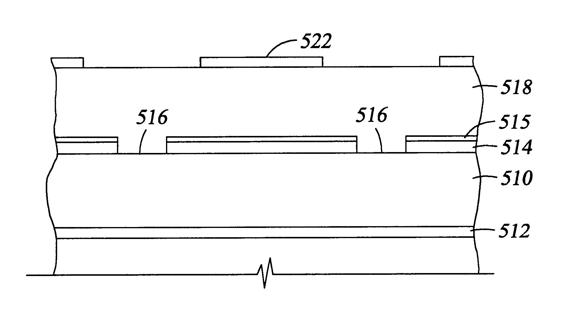
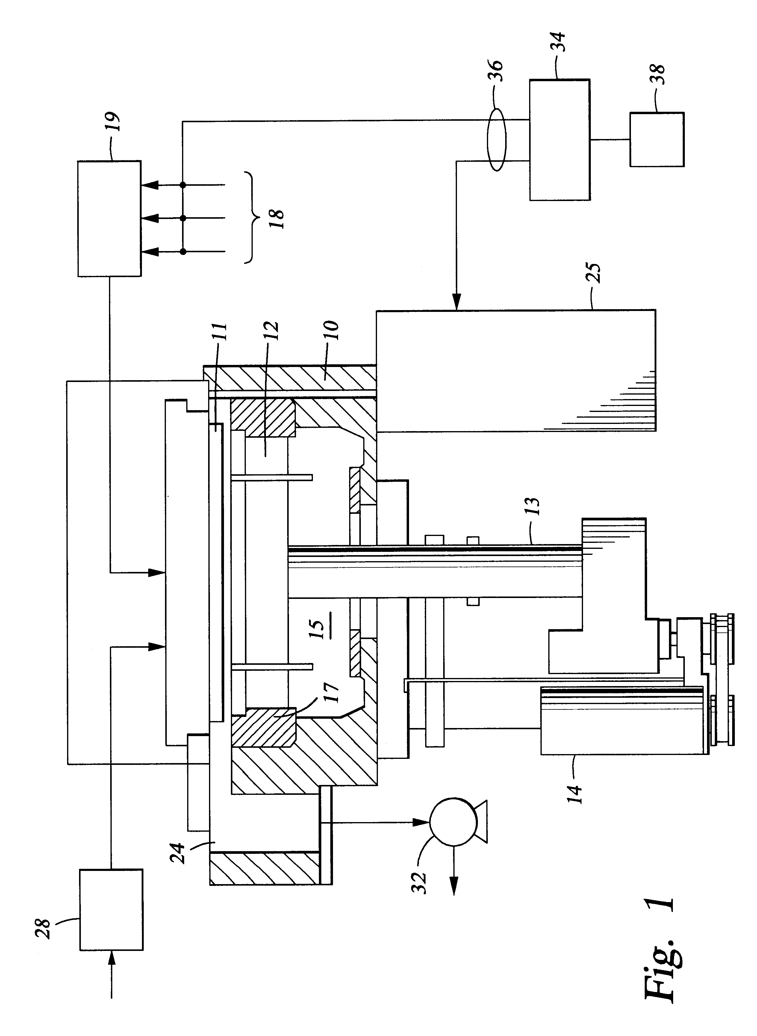
The following examples demonstrate plasma treatment of a deposition of organosilane or organosiloxane films having excellent barrier properties. These examples were undertaken using a chemical vapor deposition chamber, and in particular, a "CENTURA DxZ" system which includes a solid-state RF matching unit with a two-piece quartz process kit, both fabricated and sold by Applied Materials, Inc., Santa Clara, Calif.

Silicon Oxycarbide Surface Treatment Process

An oxidized trimethylsilane film was deposited at a chamber pressure of 4.0 Torr and a temperature of 350.degree. C. from reactive gases which were flowed into the reactor as follows:

The substrate was positioned 220 millimeters from the gas distribution showerhead and 600 W of high frequency power (13.56 MHz) was applied to the showerhead for plasma enhanced deposition of an oxidized trimethylsilane layer at an observed rate of about 7000 .ANG. / minute. The substrate was then spaced from the gas distribution showerhead at a distance...


PUM

PropertyMeasurementUnit
poweraaaaaaaaaa
chamber pressureaaaaaaaaaa

Abstract

A method is provided for processing a substrate including treating a surface of a dielectric layer comprising silicon and carbon by exposing the dielectric layer comprising silicon and carbon to a plasma of an inert gas, and depositing a photoresist on the dielectric layer comprising silicon and carbon. The dielectric layer may comprise a first dielectric layer comprising silicon, carbon, and nitrogen, and a second layer of nitrogen-free silicon and carbon containing material in situ on the first dielectric layer, and a third dielectric layer comprising silicon, oxygen, and carbon on the second dielectric layer.

Description

BACKGROUND OF THE DISCLOSURE1. Field of the InventionThe invention relates to the fabrication of integrated circuits and to a process for depositing dielectric layers on a substrate and the structures formed by the dielectric layer.2. Description of the Related ArtOne of the primary steps in the fabrication of modern semiconductor devices is the formation of metal and dielectric layers on a substrate by chemical reaction of gases. Such deposition processes are referred to as chemical vapor deposition or CVD. Conventional thermal CVD processes supply reactive gases to the substrate surface where heat-induced chemical reactions take place to produce a desired layer.Semiconductor device geometries have dramatically decreased in size since such devices were first introduced several decades ago. Since then, integrated circuits have generally followed the two year / half-size rule (often called Moore's Law), which means that the number of devices that will fit on a chip doubles every two ye...

Claims


Application Information

Patent Timeline
Patent Type & Authority Patents(United States)
IPC IPC(8): G03F7/16H01L21/02H01L21/768H01L21/70H01L21/312H01L21/311
CPCC23C16/325C23C16/401G03F7/16H01L21/3105H01L21/31144H01L21/3148H01L21/7681H01L21/76826H01L21/76828H01L21/76832H01L21/312Y10S257/914H01L21/022H01L21/02271H01L21/02126H01L21/02167H01L21/0234
Inventor XU, PINGXIA, LI-QUNDWORKIN, LARRY A.NAIK, MEHUL
Owner APPLIED MATERIALS INC
Why Eureka
Try Eureka