Combined multiplexer and switched gain circuit

a multiplexer and switching gain technology, applied in the field of multiplexers, can solve the problems of extreme care to maintain the accuracy of the signal, the effect of reducing circuit components in receivers of this type is limited, and the cost of digital circuit components is very high at high frequencies

Inactive Publication Date: 2004-01-06
NORTHROP GRUMMAN SYST CORP
View PDF10 Cites 17 Cited by
  • Summary
  • Abstract
  • Description
  • Claims
  • Application Information

AI Technical Summary

Problems solved by technology

However, digital circuit components become very expensive at high frequencies.
Further, for those digital systems that process both radio frequency (RF) and intermediate frequency (IF) signals, extreme care must be taken to maintain the accuracy of the signal, especially for waveforms employing complex modulation.
However, receivers of this type have been limited in their effectiveness for reducing circuit components, reducing the size and cost of IF sampling circuits, and maintaining signal fidelity at high frequencies.
The '831 patent offers improvements for analog-to-digital conversion, but does not address the multiplexing architecture for high frequency.
Further, combining all of the functions as is done in the '831 patent onto a single chip slows the speed of the signal throughput and compromises the isolation between the primary and diversity channels.
This design provides good isolation, but drives up the cost of implementation.

Method used


Image

  • Combined multiplexer and switched gain circuit
  • Combined multiplexer and switched gain circuit
  • Combined multiplexer and switched gain circuit

Examples


Embodiment Construction

The following discussion of the invention directed to a variable gain amplifier and multiplexer provided on a common integrated circuit chip for a dual diversity receiver system is merely exemplary in nature, and is in no way intended to limit the invention or its applications or uses. For example, the multiplexer and amplifier are employed in conjunction with a diversity receiver system in a cellular base station. However, as will appreciated by those skilled in the art, the amplifier and multiplexer of the present invention can be employed in other analog or digital processing systems.

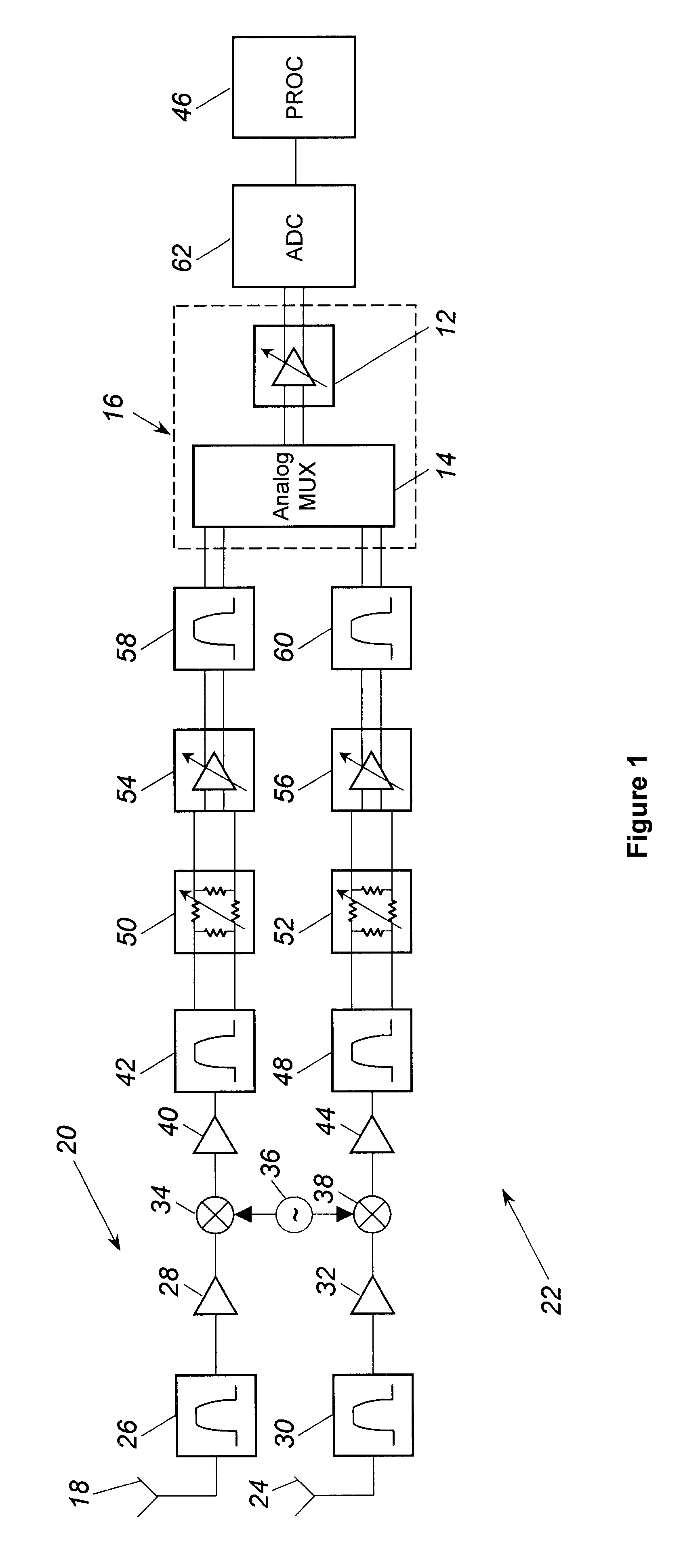
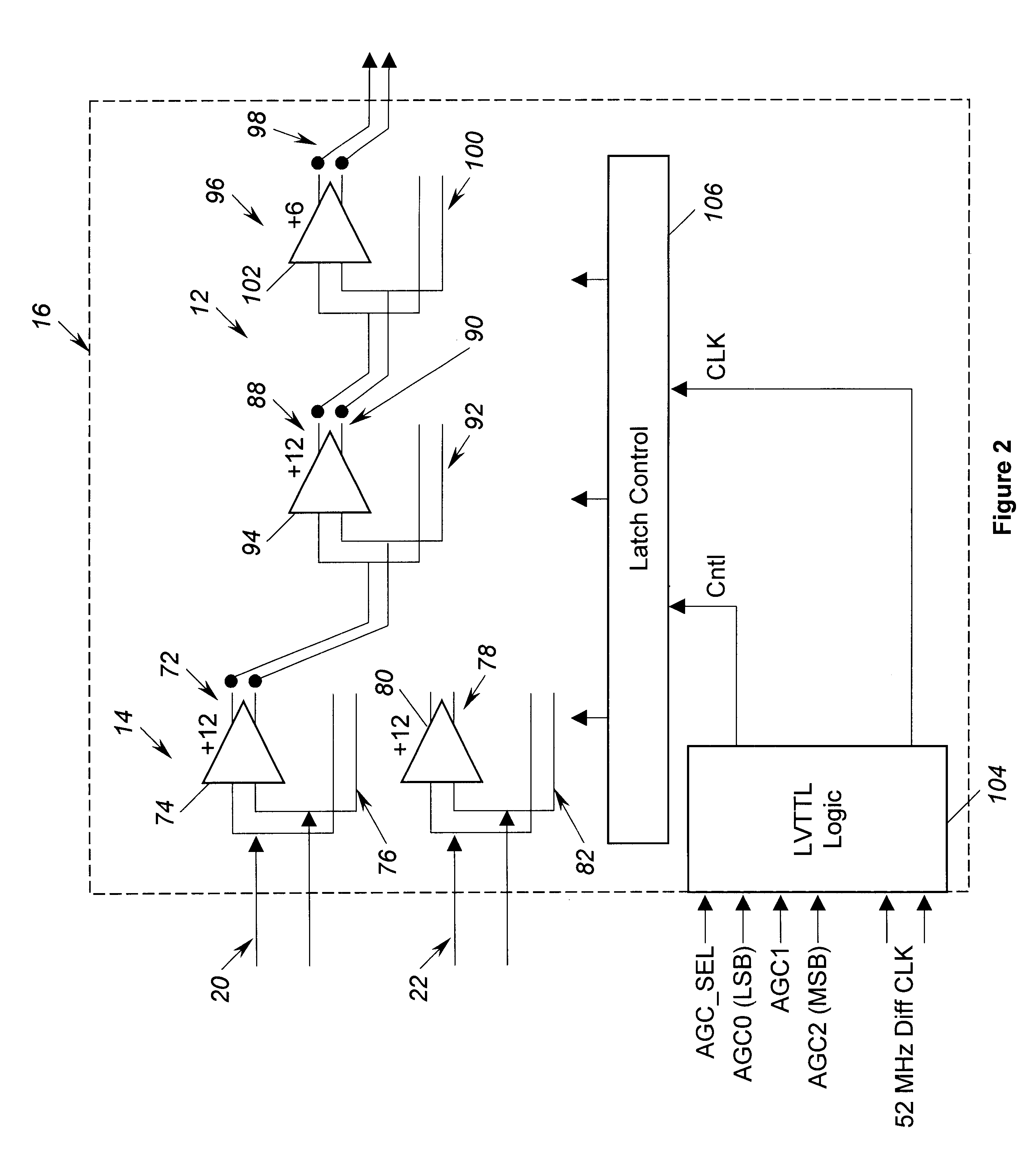
FIG. 1 is a schematic block diagram of a diversity receiver system 10 for a cellular telephone base station, according to an embodiment of the present invention. As will be discussed in detail below, the system 10 employs a VGA 12 and an analog multiplexer 14 formed on a common RF integrated circuit (IC) chip 16, according to an embodiment of the present invention. The system 10 includes a primary ch...


PUM


Abstract

A combined multiplexer and switched gain circuit (250) that selectively multiplexes differential analog signals from a primary channel (20) and a diversity channel (22) in a diversity receiver system (10) to a single output. The circuit (250) is based on a current mode logic design where a plurality of separate conduction paths (278-284) are provided between a voltage line (266) and a current source (268). An output line (264) of the circuit (250) is coupled to each conduction path (278-284) so that the differential analog signals from the primary channel (20) and the diversity channel (22) can be selectively outputted to the circuit (250). Each conduction path (278-284) includes a gain device, such as degenerative resistor, that provides signal gain or no signal gain for that conduction path (278-284). Control signals are selectively applied to switching devices (310-324) and each conduction path (278-284) so that the conduction path (278-284) can be independently selected to provide the multiplexing.

Description

1. Field of the InventionThis invention relates generally to a multiplexer for multiplexing analog signals from a primary channel and a diversity channel in a diversity receiver and, more particularly, to a combined multiplexer and switched gain circuit for multiplexing differential analog signals from a primary channel and a diversity channel in a diversity receiver, where the multiplexer provides a gain path and a no-gain path for both the primary channel signals and the diversity channel signals.2. Discussion of the Related ArtHistorically, communications systems sampled analog signals to provide signal processing in the system. Modern trends generally represent signals in communications systems as time sampled digital data signals. Because of the availability of very high frequency circuits, it has become possible to process digital signals at higher and higher frequencies into the 100's of MHz. Digital signal processing offers the advantages of flexibility for change, absolute ...

Claims


Application Information

Patent Timeline
Patent Type & Authority Patents(United States)
IPC IPC(8): H03M1/18H03M1/12H03G3/10H03K17/00H03G3/20H03G3/30H03K17/62H04B7/08
CPCH03M1/18H03M1/1225
Inventor HARBERTS, HARRY S.
Owner NORTHROP GRUMMAN SYST CORP
Why Eureka
Try Eureka