Data line driving circuit of electro-optical panel, control method thereof, electro-optical device, and electronic apparatus

a technology of driving circuit and data line, applied in the direction of electric digital data processing, instruments, computing, etc., can solve the problems of large circuit scale of address decoder, increased power consumption, and inability to realize circuit scal

Inactive Publication Date: 2004-01-27
TCL CHINA STAR OPTOELECTRONICS TECH CO LTD
View PDF11 Cites 59 Cited by
  • Summary
  • Abstract
  • Description
  • Claims
  • Application Information

AI Technical Summary

Benefits of technology

According to the present invention, since the shift register section is divided into blocks by a plurality of shift registers, it is possible to selectively cause a necessary shift register to operate. Consequently, it is possible to reduce power consumption.
Also, in the above-described invention, preferably, the enable signal generation section causes, based on the determination result of the determination section, the enable signal to become non-active when a predetermined number of dots in which the data values match between horizontal lines continue. According to the present invention, unless a certain amount of mismatching of the data values continues, the logic level of the enable signal does not change, and consequently, the power consumption required to drive the enable signal can be reduced. In a case where a match and a mismatch of the data values repeat in dot units, since matches have not occurred continuously, the enable signal does not become non-active, and no electric power is consumed to drive the enable signal, whereas when the number of dots in which a match occurs exceeds a predetermined number, the enable signal becomes non-active, making it possible to reduce the electric power required to drive the image data.

Problems solved by technology

However, a problem arises that the circuit scale of the address decoder becomes large, and as a consequence, the power consumption is increased.
In particular, a problem arises that even if an attempt to form an address decoder on a device substrate is made by using thin-film transistors (hereinafter referred to as "TFTs"), the circuit scale thereof is too large to be realized.
On the other hand, in order to perform sampling, it is necessary to cause the shift register to operate in order to generate a sampling signal by supplying a clock signal thereto, and parasitic capacitance occurs in the wiring which supplies the clock signal.
Since the wiring acts as a capacitive load, in order to supply the clock signal at a sufficient through rate, a large amount of electric power is required.
On the other hand, parasitic capacitance occurs in the wiring which supplies the image data.
Since the wiring acts as a capacitive load, in order to supply the image data at a sufficient through rate, a large amount of electric power is required.
For this reason, if the control device 300 always drives the image data supply line DL, which is a capacitive load, a lot of electric power is consumed.
Also, if the logic level is changed, electric power is consumed therein.

Method used


Image

  • Data line driving circuit of electro-optical panel, control method thereof, electro-optical device, and electronic apparatus
  • Data line driving circuit of electro-optical panel, control method thereof, electro-optical device, and electronic apparatus
  • Data line driving circuit of electro-optical panel, control method thereof, electro-optical device, and electronic apparatus

Examples


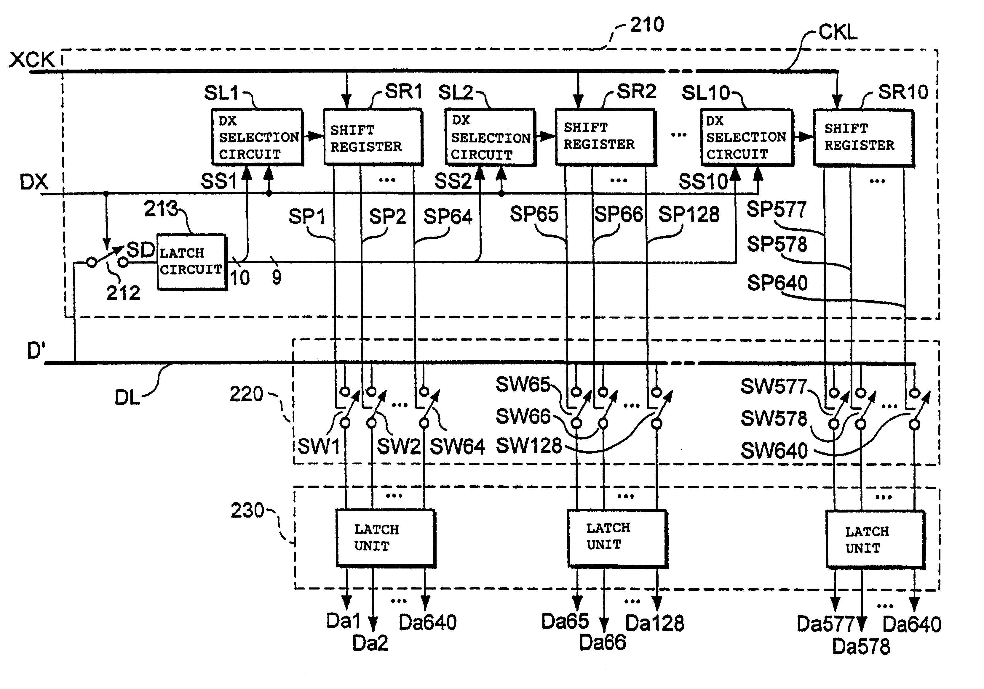
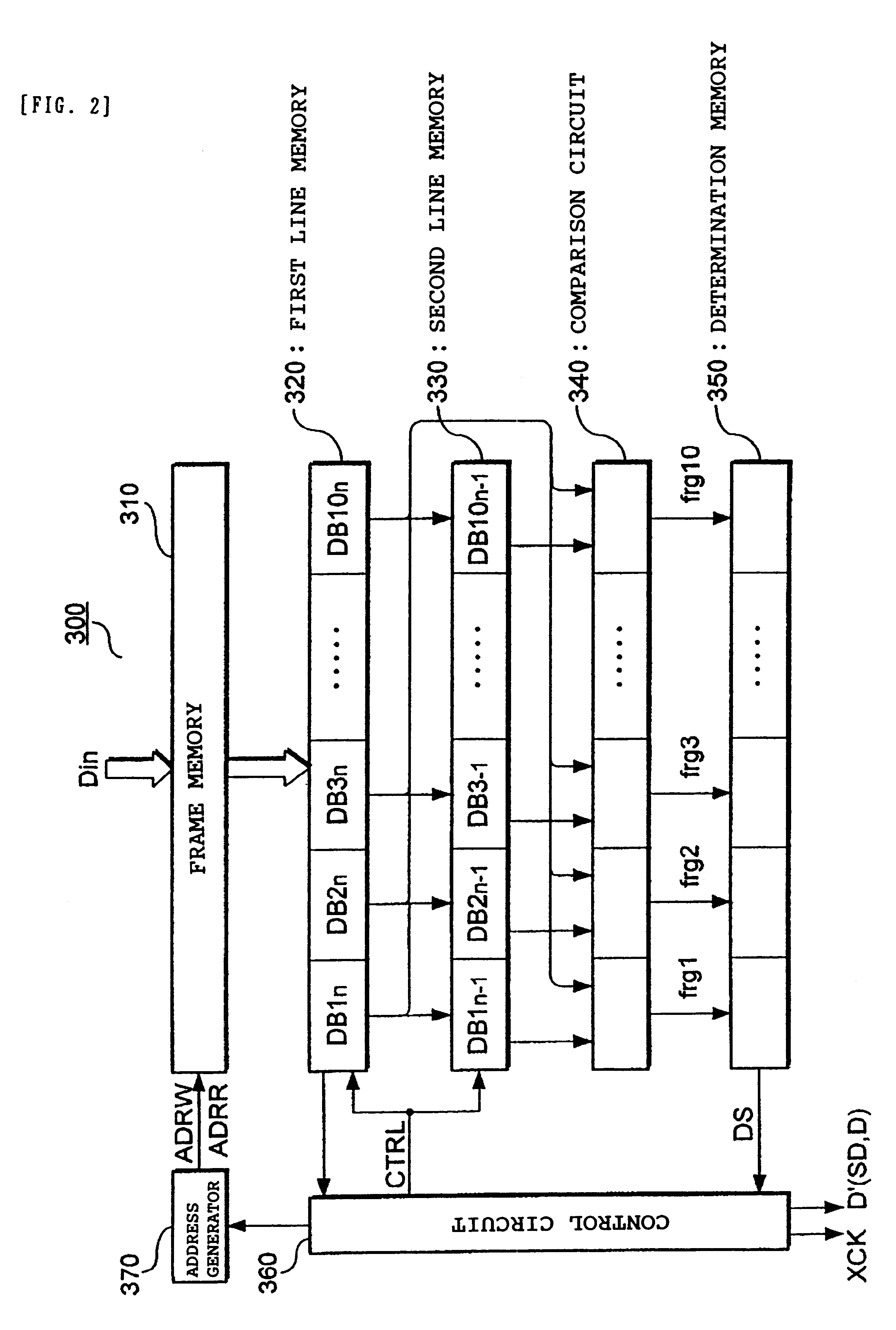
Embodiment Construction

of Liquid-crystal Device>

Next, a description is given of a case in which the liquid-crystal device described in the first embodiment and the second embodiment is applied to various electronic apparatuses.

First, a projector in which this liquid-crystal device is used as a light valve is described. FIG. 15 is a plan view showing an exemplary structure of the projector.

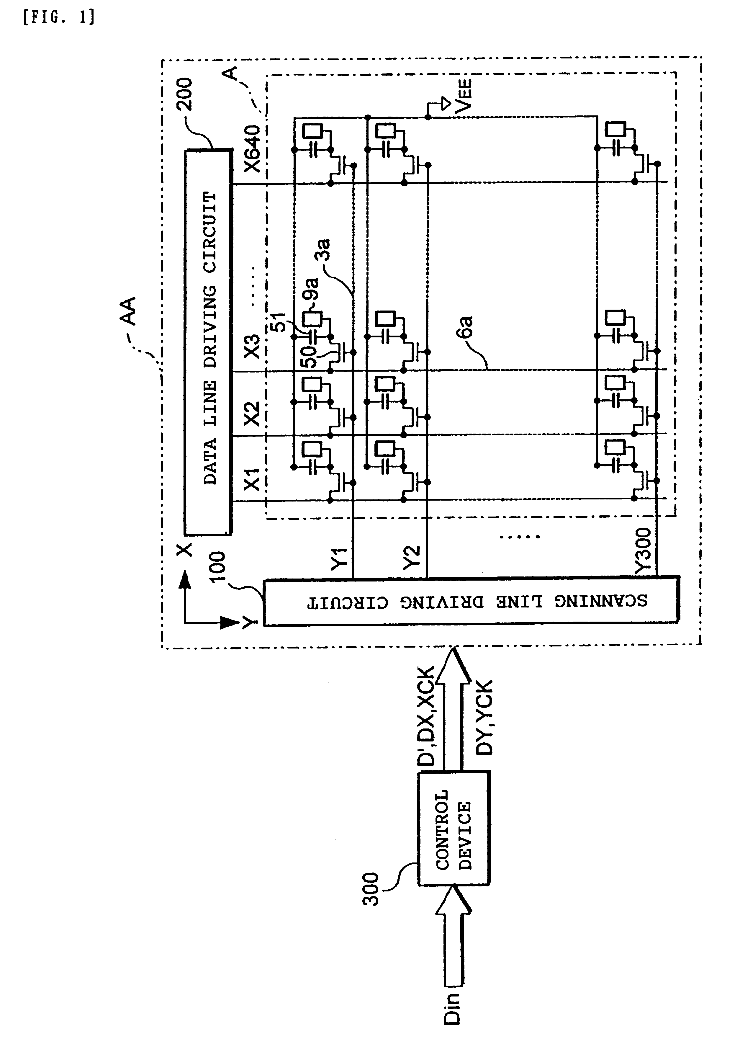
As shown in this figure, inside a projector 1100, a lamp unit 1102 formed of a white light source, such as a halogen lamp, is provided. The projected light emitted from this lamp unit 1102 is separated into three primary colors of RGB by four mirrors 1106 and two dichroic mirrors 1108, disposed inside a light guide 1104, and is made to enter liquid-crystal panels 1110R, 1110B, and 1110G as light valves corresponding to each of the primary colors.

The liquid-crystal panels 1110R, 1110B, and 1110G are formed similarly to the above-described liquid-crystal panel AA, and are driven in accordance with primary-color image infor...


PUM

PropertyMeasurementUnit
DAaaaaaaaaaa
time-divisionaaaaaaaaaa
conducting stateaaaaaaaaaa

Abstract

The disclosed invention reduces the power consumption of a liquid-crystal device. A shift register section includes DX selection circuits and shift registers, which are divided into blocks. An X clock signal is supplied to a block in which the image data values do not match between horizontal lines which are adjacent in a data time-series manner, and is not supplied to a block in which the image data values match. In addition, for the block in which the image data values match, the image data, which forms time-division data becomes non-active, and the previous data value is maintained. For this reason, it is possible to reduce electric power for driving an X clock signal supply line and an image data supply line.

Description

1. Field of InventionThe present invention relates to a data line driving circuit of an electro-optical panel, a control method thereof, an electro-optical device using these, and an electronic apparatus.2. Description of Related ArtA conventional electro-optical device, for example, an active-matrix-type liquid-crystal display device, mainly includes a device substrate, on which a switching device is provided via pixel electrodes arrayed in a matrix, an opposing substrate, on which color filters, etc., are provided, and a liquid crystal which is provided between these two substrates. In such a structure, when a scanning line signal is applied to the switching device via scanning lines, the switching device is placed in a conducting state. During this conducting state, when an image signal is applied to the pixel electrode via data lines, a predetermined charge is stored in the liquid-crystal layer between the pixel electrode and the opposing electrode (common electrode). After the ...

Claims


Application Information

Patent Timeline
Patent Type & Authority Patents(United States)
IPC IPC(8): G09G3/36G02F1/133G09G3/20
CPCG09G3/3688G09G2310/0286G09G2330/021G09G3/36
Inventor OZAWA, TOKURO
Owner TCL CHINA STAR OPTOELECTRONICS TECH CO LTD
Why Eureka
Try Eureka