Under bump metallurgy for lead-tin bump over copper pad

a technology of leadtin and bumping, which is applied in the direction of manufacturing tools, soldering equipment, semiconductor/solid-state device details, etc., can solve the problems of affecting the performance and reliability of the chip-to-package interconnection, bumping significantly increasing the density of i/o connections, and bumping reducing the footprint of the packag

Inactive Publication Date: 2004-03-09
INTEL CORP
View PDF4 Cites 33 Cited by
  • Summary
  • Abstract
  • Description
  • Claims
  • Application Information

AI Technical Summary

Problems solved by technology

However, the performance and the reliability of the chip-to-package interconnection may be affected since wirebonding requires the routing of all the input / output (I / O) connections to the edges of the chip.
First, bumping significantly increases the density of the I / O connections.
Third, bumping decreases the footprint of the package.
However, during thermal cycling, the Tin in the bump tends to migrate through cracks or other defects in the UBM and react with the Copper in the bond pad to form an intermetallic compound which may cause shorting of the interconnects thereby leading to premature failure of the interconnect.

Method used


Image

  • Under bump metallurgy for lead-tin bump over copper pad
  • Under bump metallurgy for lead-tin bump over copper pad

Examples


Embodiment Construction

In the following description, numerous particular details, such as specific materials, dimensions, and processes, are set forth in order to provide a thorough understanding of the present invention. However, one skilled in the art will realize that the invention may be practiced without these particular details. In other instances, well-known semiconductor equipment and processes have not been described in particular detail so as to avoid obscuring the present invention.

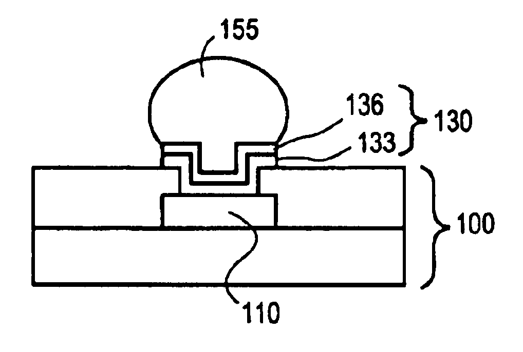
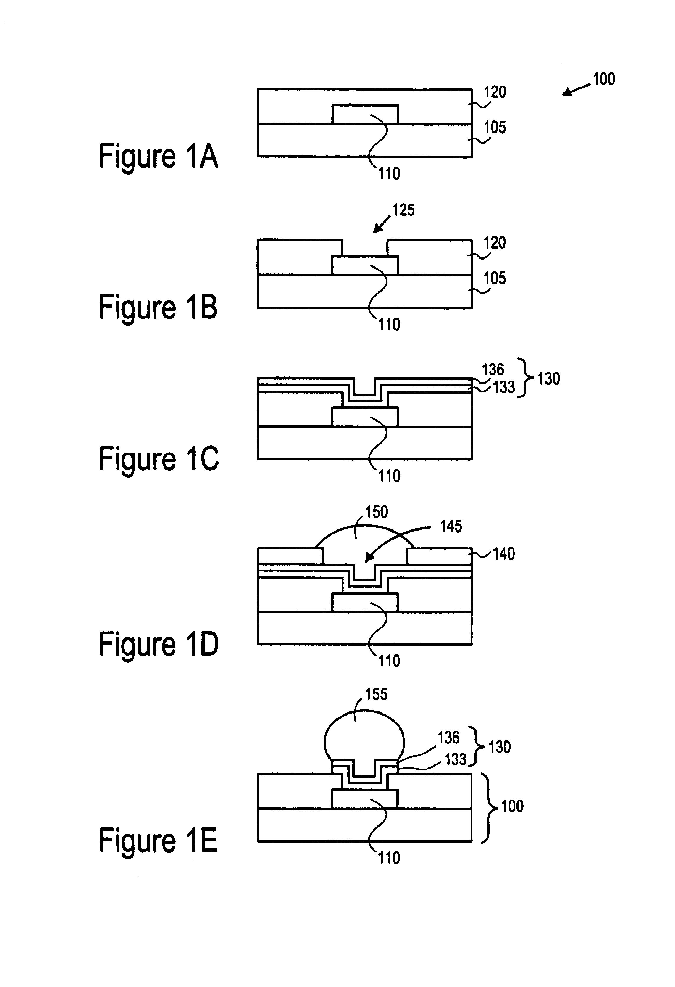
The present invention includes a method of forming a more reliable under bump metallurgy (UBM) and a UBM that is more reliable. The method of the present invention suppresses the diffusion of Tin from a solder bump to an underlying Copper bond pad, minimizes the formation of a Copper-Tin (Cu:Sn) intermetallic compound, and prevents shorting of interconnects. The UBM of the present invention may include Aluminum with an alloying element such as Magnesium.

An embodiment of a method of the present invention is shown in F...


PUM

PropertyMeasurementUnit
thicknessaaaaaaaaaa
thicknessaaaaaaaaaa
thicknessaaaaaaaaaa

Abstract

The present invention describes a method including providing a component, the component having a bond pad; forming a passivation layer over the component; forming a via in the passivation layer to uncover the bond pad; and forming an under bump metallurgy (UBM) over the passivation layer, in the via, and over the bond pad, in which the UBM includes an alloy of Aluminum and Magnesium.The present invention also describes an under bump metallurgy (UBM) that includes a lower layer, the lower layer including an alloy of Aluminum and Magnesium; and an upper layer located over the lower layer.

Description

1. Field of the InventionThe present invention relates to the field of semiconductor integrated circuit (IC) manufacturing, and more specifically, to a method of forming a more reliable under bump metallurgy (UBM) and an UBM that is more reliable.2. Discussion of Related ArtChip-to-package interconnections have traditionally involved wirebonding which is very cost-effective. Wirebonding is the use of very fine metal wires to join contacts on a chip with corresponding contacts on a package. As the size of a transistor is reduced, the size of the chip-to-package interconnection also has to be scaled down. However, the performance and the reliability of the chip-to-package interconnection may be affected since wirebonding requires the routing of all the input / output (I / O) connections to the edges of the chip.Solder bumping is the use of reflowable solder balls to join contacts on the chip with corresponding contacts on the package. Solder bumping requires that the chip be flipped over ...

Claims


Application Information

Patent Timeline
Patent Type & Authority Patents(United States)
IPC IPC(8): B23K1/20B23K1/00H01L21/60H01L23/485H01L21/02H01L23/48C22C21/06
CPCB23K1/0016C22C21/06H01L24/03H01L24/11B23K1/20Y10T428/12743B23K2201/42H01L2224/03912H01L2224/0401H01L2224/1147H01L2224/13023H01L2224/131H01L2924/01003H01L2924/01006H01L2924/01007H01L2924/01012H01L2924/01013H01L2924/01014H01L2924/01022H01L2924/01025H01L2924/01027H01L2924/01028H01L2924/01029H01L2924/01032H01L2924/0104H01L2924/01046H01L2924/0105H01L2924/01082H01L2924/01327H01L2924/014H01L2924/05042H01L2924/14Y10T428/12736Y10T428/12806Y10T428/265H01L2924/00013H01L2924/01023H01L2924/01024H01L2924/01033H01L2924/01072Y10T428/12701Y10T428/1275Y10T428/12903Y10T428/12486H01L2224/13099H01L2224/0361B23K2101/42
Inventor MOON, PETER K.MA, ZHIYONGDATTA, MADHAV
Owner INTEL CORP
Why Eureka
Try Eureka