Method of biasing the photodiodes of a matrix sensor through associated pixels thereof

a matrix sensor and photodiode technology, applied in the field of method of biasing the photodiodes of a matrix sensor through associated pixels thereof, can solve the problems of inapplicability of the solution represented in fig. 5 and the inability to control the cathodes of each photodiode individually, and the control method has some disadvantages

Inactive Publication Date: 2004-03-16
COMMISSARIAT A LENERGIE ATOMIQUE ET AUX ENERGIES ALTERNATIVES
View PDF7 Cites 11 Cited by
  • Summary
  • Abstract
  • Description
  • Claims
  • Application Information

AI Technical Summary

Benefits of technology

From a certain threshold on, the space variation of the photodiode operating point has the effect of reducing sensor performance because the optimal biasing range is reduced thereby.
The depolarization space variation amplitude is all the greater since the number of sides whereon the P.sup.++ ohmic contact 12 can be implanted is reduced.
This difficulty could be obviated by replacing one or several photodiodes with a P.sup.++ contact. However, this would have the effect of increasing the number of the sensor's blind pixels.
First of all, it significantly increases the number of manufacturing steps'. Indeed, it is necessary to produce P.sup.++ -type areas, then to pick up ohmic contacts in these areas.
The invention eliminates the need to keep the ohmic contact 12. Thus, a set of coplanar photodetectors can be obtained, together composing an image sensor circuit, each photodetector composing in general one image pixel, wherein the value of the signal output by one of the photodetectors is not modified or not much modified by the value of the signal output by other photodetectors of the sensor. It aims at obtaining a detector circuit with greater density per unit area, i.e. with a greater number of photodetectors per unit area of a detector circuit. Finally, it aims at simplifying the manufacturing of a detector circuit.

Problems solved by technology

On the other hand, the cathodes of each photodiode cannot be controlled individually.
However, this solution represented in FIG. 5 is not always applicable.
However, this control method has some disadvantages that will be approached below.

Method used


Image

  • Method of biasing the photodiodes of a matrix sensor through associated pixels thereof
  • Method of biasing the photodiodes of a matrix sensor through associated pixels thereof
  • Method of biasing the photodiodes of a matrix sensor through associated pixels thereof

Examples


Embodiment Construction

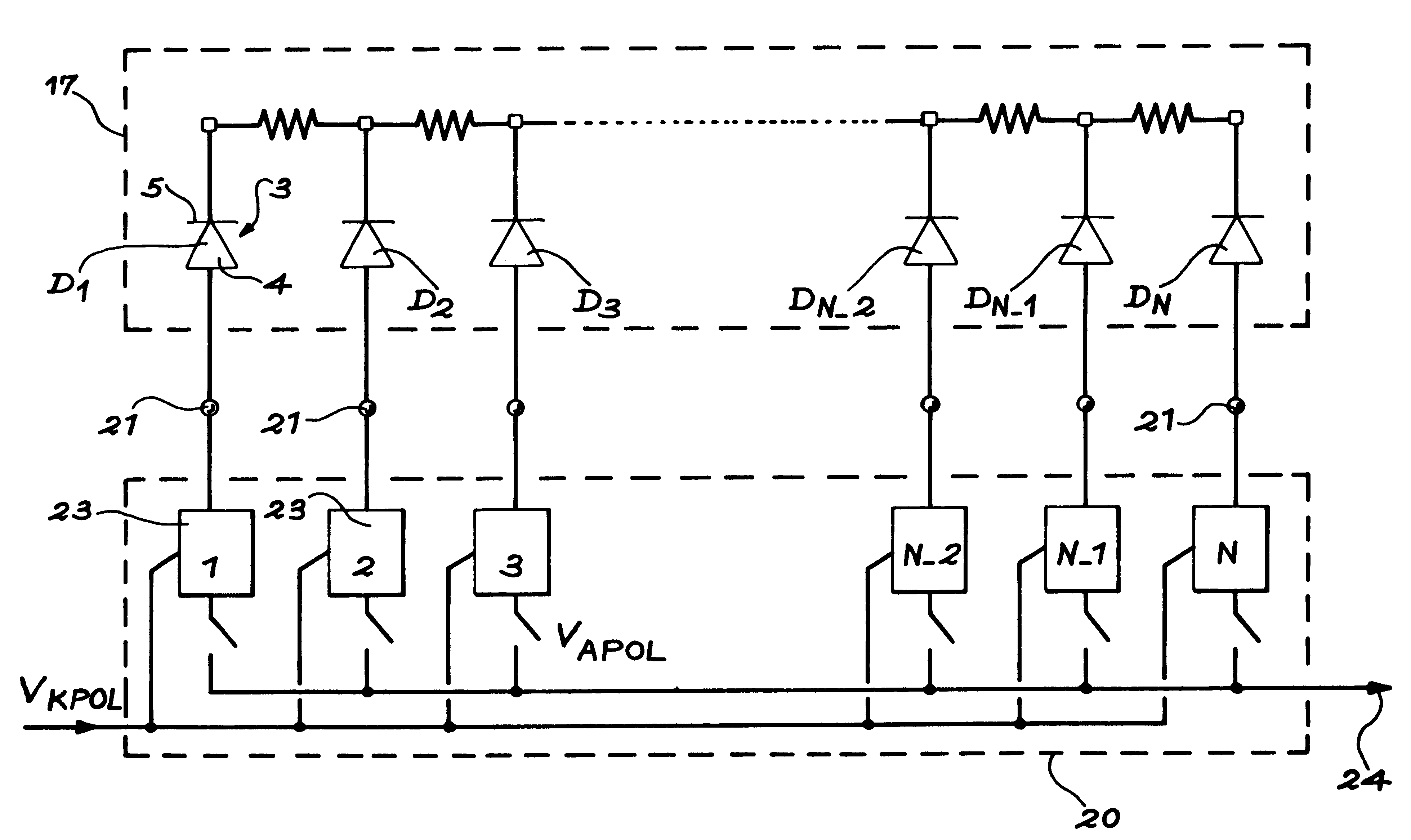
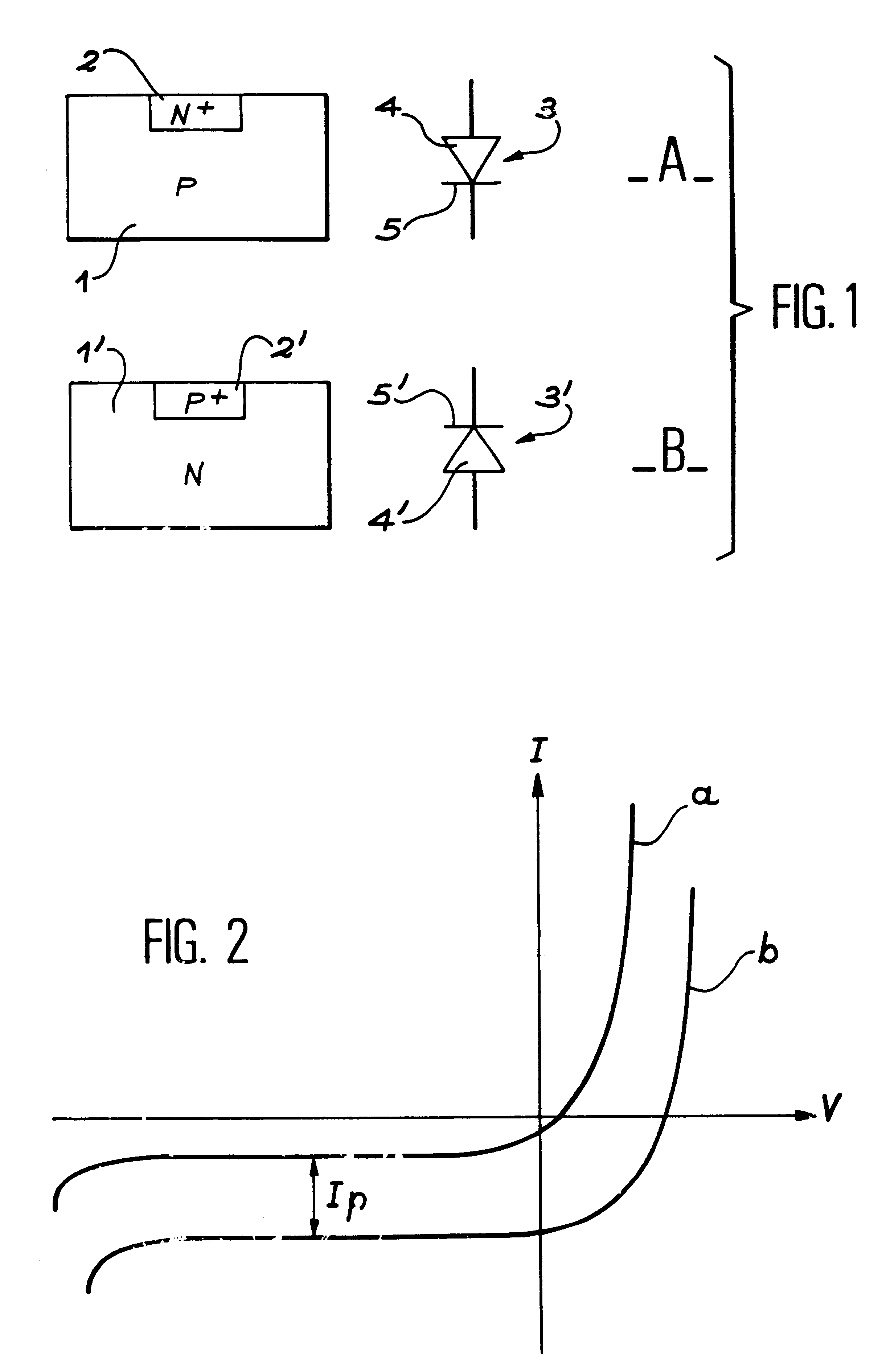
As it has been seen above, the invention consists in imposing, by control diode anode voltage control, the cathode voltage of each photodiode so as to equalize the apparent impedance of each photodiode among them.

Advantageously, on the detector circuit, diodes will be implanted that can be forward biased and one electrode of which will be permanently coupled to a constant voltage source through the read circuit.

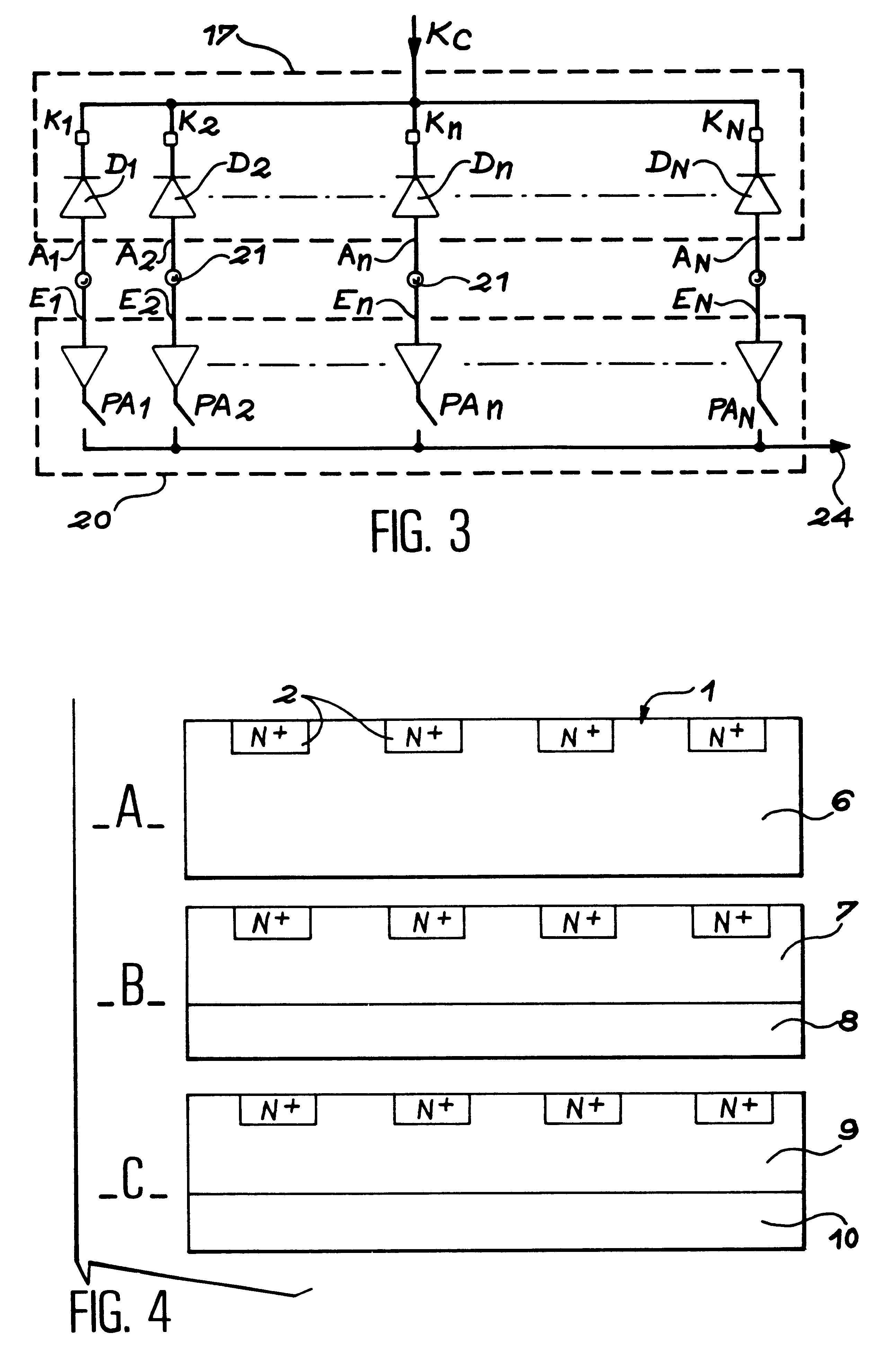
Geometrical implantation modes of such diodes are represented in FIGS. 10 and 11.

FIG. 10 represents the case of a linear strip of photodetectors where all the space required for implanting control diodes is available.

In this case, control diodes 18 can be aligned on a line parallel to the photodiode 19 implantation line. In the example represented in FIG. 10, each control diode 18 is located in alignment with a photodiode 19.

In this case, it is also possible to provide two lines of control diodes located on either side of the photodiode line as represented in FIG. 17 part B, ...


PUM


Abstract

An image sensor comprises a detector circuit (17) with detector diodes (3), which are reverse biased during image sensing. It is characterized in that the cathode voltage of the detector diodes is controlled by forward biasing detector circuit (17) diodes via the read circuit (20). The control diodes can be dedicated diodes or forward biased photodetector diodes. In the latter case, a picture is taken in several sequences.

Description

This invention relates to the field of electromagnetic radiation, in particular visible or infrared radiation, detector networks. The field is limited more particularly to image sensors (ref. [1], [2] of the appended list) composed of a detector circuit interconnected to a read circuit. It relates to a device and method of biasing such photodetectors.TECHNOLOGICAL BACKGROUNDOverview of PhotodetectionA photodiode is a semiconductor device, which, when illuminated by sufficient energy radiation, outputs a photocurrent by generating electron-hole pairs. Two categories of photodiodes can be produced, according to the type of junction and substrate doping, the N-type junction on P-type semiconductor material and its equivalent, a P junction on N material.Only the case of N photodiodes on P will be discussed hereafter. All the principles that will be presented are easily transposed to type-P photodiodes on N substrate by a person skilled in the art.The detector circuit is generally formed...

Claims


Application Information

Patent Timeline
Patent Type & Authority Patents(United States)
IPC IPC(8): H04N3/15H04N5/365H04N5/374H04N5/378
CPCH04N5/33H04N5/3658H04N5/3741H04N5/378H04N25/677H04N25/766H04N25/75
Inventor PANTIGNY, PHILIPPEMARTIN, JEAN-LUCHAMELIN, REGISPALTRIER, SYLVAIN
Owner COMMISSARIAT A LENERGIE ATOMIQUE ET AUX ENERGIES ALTERNATIVES
Why Eureka
Try Eureka