Spin-valve structure and method for making spin-valve structures

a spin-valve structure and spin-valve technology, applied in the field of spin-valve structure and method for making spin-valve structures, can solve the problems of low field sensing, current shunting, signal loss,

Inactive Publication Date: 2004-04-13
INTERUNIVERSITAIR MICRO ELECTRONICS CENT (IMEC VZW)
View PDF1 Cites 18 Cited by
  • Summary
  • Abstract
  • Description
  • Claims
  • Application Information

AI Technical Summary

Benefits of technology

A first aim of the present invention is to provide novel magnetic devices capable of high magnetoresistive signals and high sensitivities at low fields.
A further aim of the present invention is to provide a novel method for producing a magnetic sensor capable of sensing high magnetoresistive signals and having high sensitivities at low fields.
Another aim of the present invention is to provide a novel low-cost fabrication method for spin-valve structures.
In a preferred embodiment, there is an electrical barrier between the first free ferromagnetic layer and the semiconductor surface. Said electrical barrier can be a Schottky Barrier or a Tunnel Barrier. Such electrical barrier can be formed while depositing said first free ferromagnetic layer on said semiconductor surface and can prevent shunting currents and protect said spin-valve structure against electrostatic discharge. This barrier however is weak enough to provide electrical contact if necessary during deposition.
The present invention also relates to a spin-valve structure comprising a first and a second free ferromagnetic layers and a spacer layer, preferably an antiferromagnetic or a metal or semimetal or conductive semiconductor layer, positioned between said first and said second free ferromagnetic layers wherein said first free ferromagnetic layer is positioned on a substrate forming a barrier with a ferromagnetic layer being positioned thereon. This barrier is such that it can prevent shunting currents or other forms of electrical transport from the substrate to the magnetic layers during operation of the spin-valve structure while allowing for electrical contact if necessary during deposition of the ferromagnetic layer on the substrate. Such substrate can also be a polymer material.

Problems solved by technology

Due to the above mentioned high saturation fields, these electrodeposited / electroplated multilayers are unattractive for low field sensing.
If this seed layer cannot be removed, problems of current shunting and signal loss occur when measuring the magnetoresistive properties of the electrodeposited or electroplated materials.

Method used


Image

  • Spin-valve structure and method for making spin-valve structures
  • Spin-valve structure and method for making spin-valve structures
  • Spin-valve structure and method for making spin-valve structures

Examples


Embodiment Construction

Embodiments and examples of the invention will be described below. It is evident that the person skilled in the art will be able to imagine or make other embodiments according to the present invention, the spirit and the scope of this invention being limited only by the appended claims.

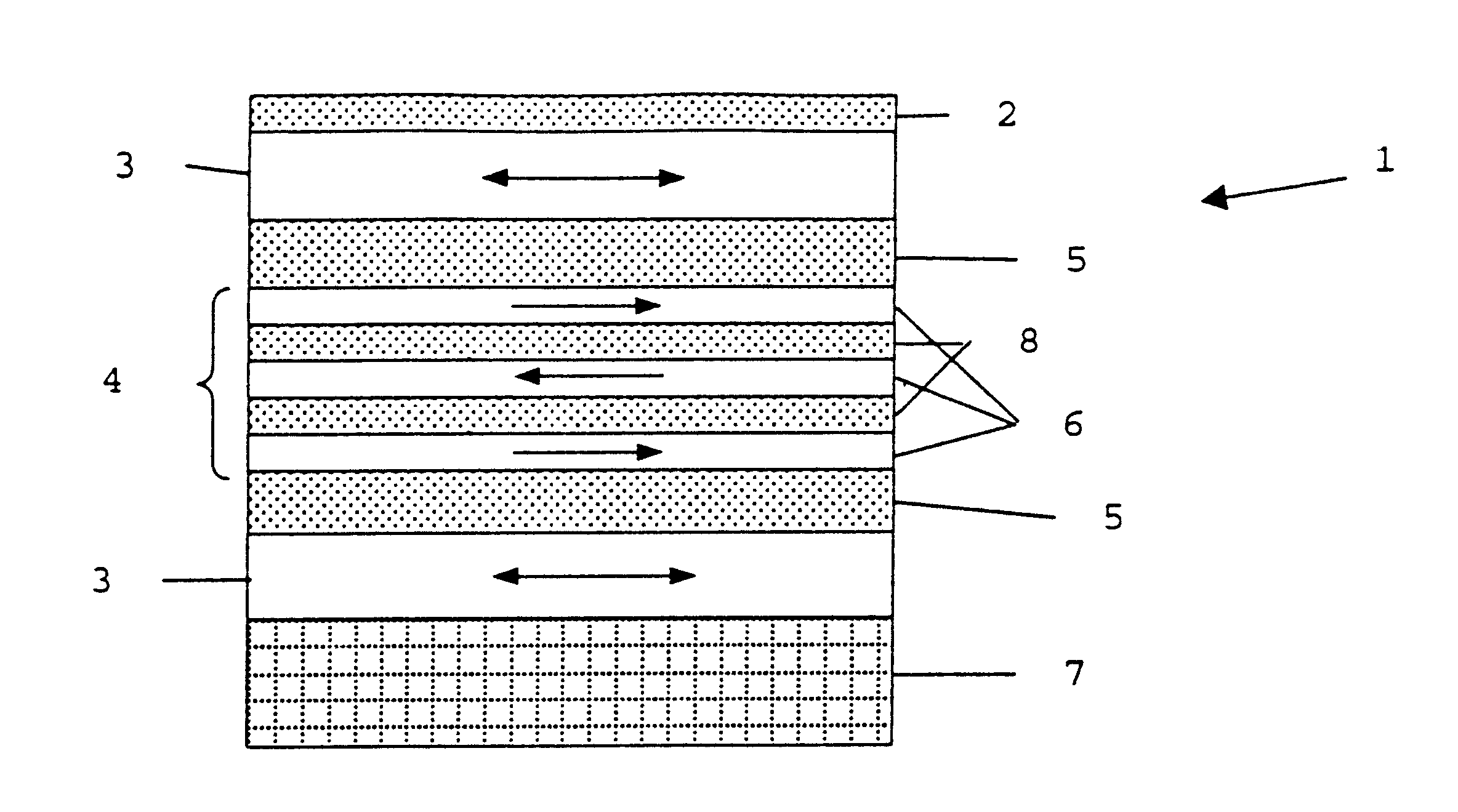
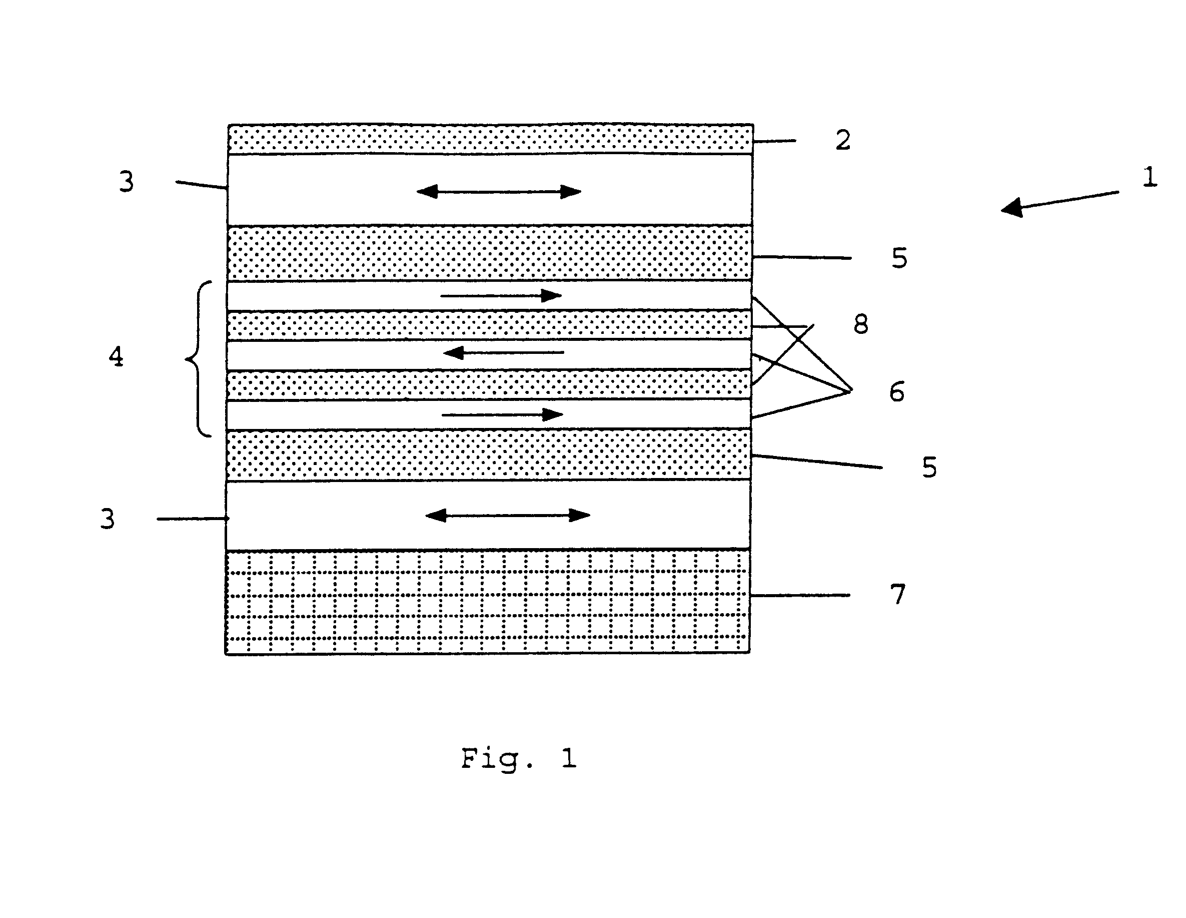
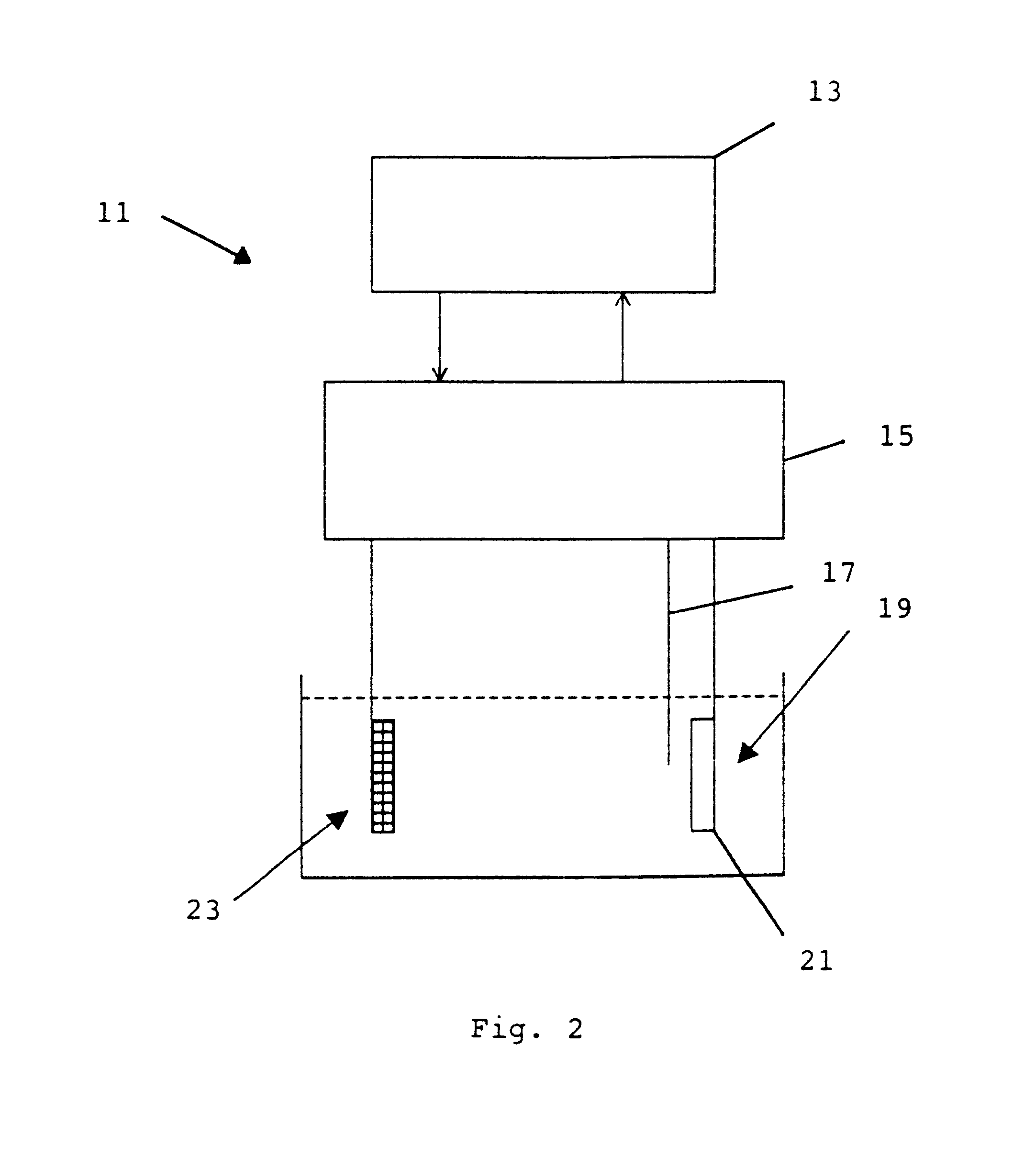
The aims of the invention are met in the present invention. A spin-valve deposited on a semiconductor substrate or any other substrate with an insulating layer between the substrate and the spin-valve results in a highly sensitive magnetic sensor. The production of a magnetic sensor can comprise the electroplating of a spin-valve structure on a substrate and can provide a sensor capable of high magnetoresistive signals and high sensitivity for low fields.

The process according to the invention thus can comprise an electrodeposition step. Electrodeposition usually takes place on a conductive seed layer, typically Cu. If this seed layer cannot be removed, problems of current shunting and signal loss occu...


PUM

PropertyMeasurementUnit
thicknessaaaaaaaaaa
electricalaaaaaaaaaa
electrical transportaaaaaaaaaa

Abstract

The present invention concerns in a first aspect a spin-valve structure having a first and a second free ferromagnetic layer and a spacer layer positioned between the first and second free ferromagnetic layer, and wherein the first free ferromagnetic layer is positioned on a substrate. In a preferred embodiment of the invention, the first free ferromagnetic layer is in direct contact with the surface of the substrate.

Description

This invention relates to the structure and fabrication of magnetic devices having a spin-valve structure.STATE OF THE ARTThe giant magnetoresistance (GMR) effect is known in the art. It is of large interest for applications in magnetoresistive read and write heads and for magnetic sensors. GMR magnetic multilayers exhibit strong coupling characteristics and thus high saturation fields. A multilayer or superlattice is a multitude of ferromagnetic and antiferromagnetic layers. The ferromagnetic layers can be coupled or uncoupled.Recently several research groups have shown that the single bath electrodeposition or electrodeposition technique, is an attractive technique for the production of GMR multilayers (W. Schwarzacher and D. S. Lashmore, Giant magnetoresistance in electrodeposited films, IEEE-Trans. Magn., 32 (1996) 3133-53). Due to the above mentioned high saturation fields, these electrodeposited / electroplated multilayers are unattractive for low field sensing. The largest sens...

Claims


Application Information

Patent Timeline
Patent Type & Authority Patents(United States)
IPC IPC(8): G01R33/06G01R33/09G11C11/56H01F41/30H01F41/26H01F10/00H01F10/32H01F41/14H01L43/00H01L43/08H01L43/12G11B5/39H01F10/08
CPCB82Y10/00B82Y40/00G01R33/093G11C11/5607H01F10/3268H01F10/3272H01F41/26H01F41/302H01L43/08H01L43/12B82Y25/00Y10T428/1157G11B5/3903G11B2005/3996G11C2211/5615G11C2211/5616Y10T428/1193H10N50/10H10N50/01
Inventor ATTENBOROUGH, KARENBOEVE, HANSBOECK, JO DECELIS, JEAN-PIERRE
Owner INTERUNIVERSITAIR MICRO ELECTRONICS CENT (IMEC VZW)
Why Eureka
Try Eureka