Method of circuit verification in digital design

a circuit verification and digital design technology, applied in the field of improved circuit verification procedures, can solve the problems affecting the operation of many eda so as to achieve the effect of increasing the workload of verification tools

Inactive Publication Date: 2004-04-27
ONESPIN SOLUTIONS
View PDF9 Cites 53 Cited by
  • Summary
  • Abstract
  • Description
  • Claims
  • Application Information

AI Technical Summary

Benefits of technology

A further advantage of the present invention is that, if the analysis yields that no reduction at all is possible for a given design and a given property, then reduced model and original design are identical. The verification task itself cannot be impaired by using the proposed method as a pre-process, and in all case studies pre-processing runtimes were negligible Furthermore, the technique can be applied in high-level equivalence checking and high-level simulation. High-level equivalence checking, for example, can be considered a special case of high-level property checking. The design specification can include two different implementations of the same circuit and the property can require functional equivalence, or the property itself can be written in a hardware description language representing a functional specification of the circuit.
is that, if the analysis yields that no reduction at all is possible for a given design and a given property, then reduced model and original design are identical. The verification task itself cannot be impaired by using the proposed method as a pre-process, and in all case studies pre-processing runtimes were negligible Furthermore, the technique can be applied in high-level equivalence checking and high-level simulation. High-level equivalence checking, for example, can be considered a special case of high-level property checking. The design specification can include two different implementations of the same circuit and the property can require functional equivalence, or the property itself can be written in a hardware description language representing a functional specification of the circuit.
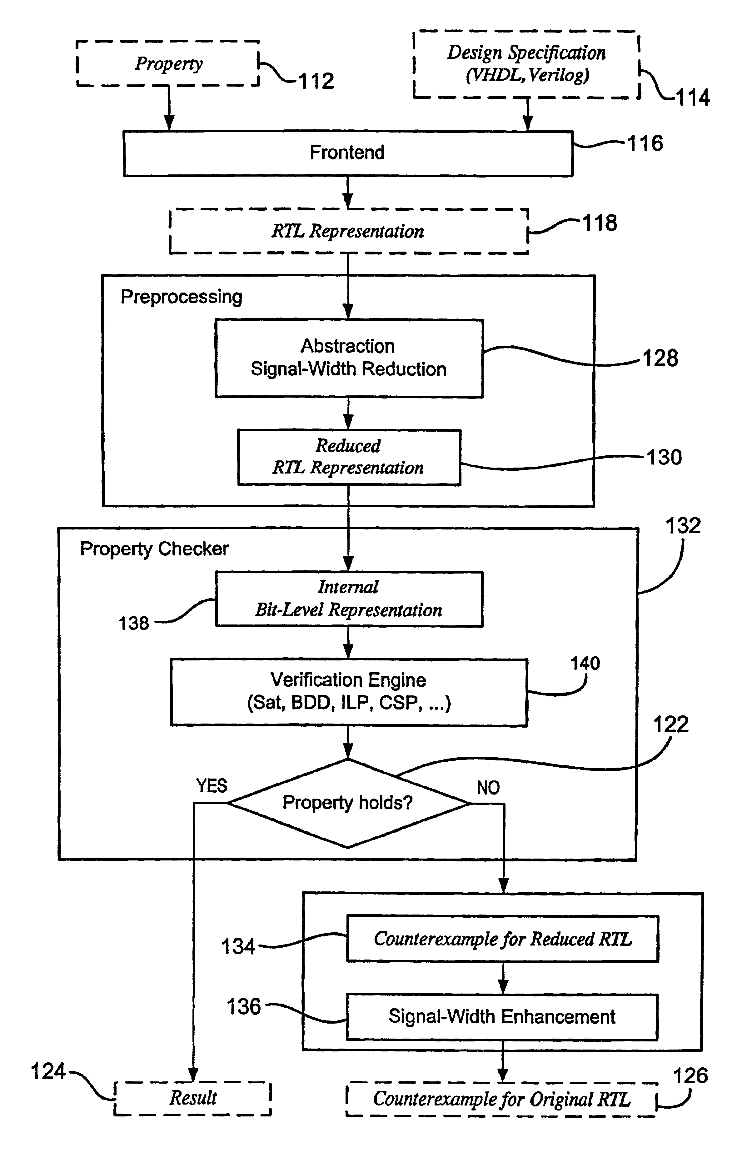
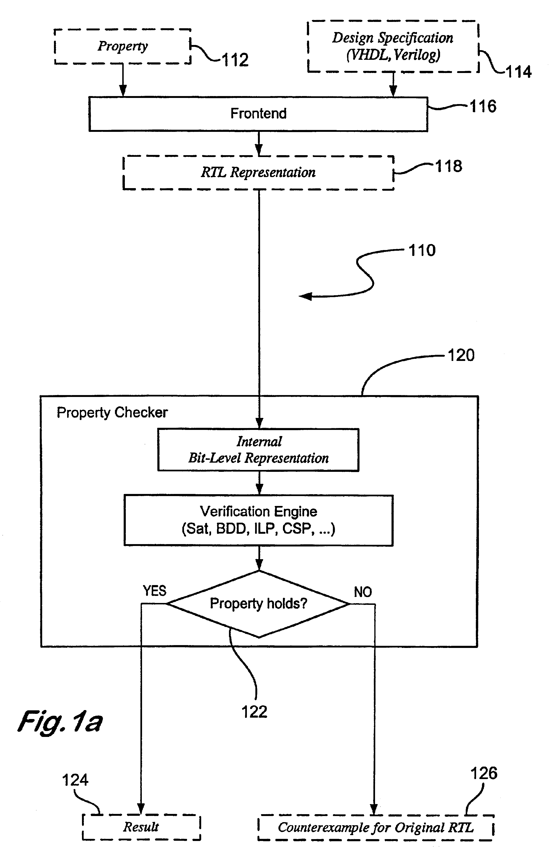
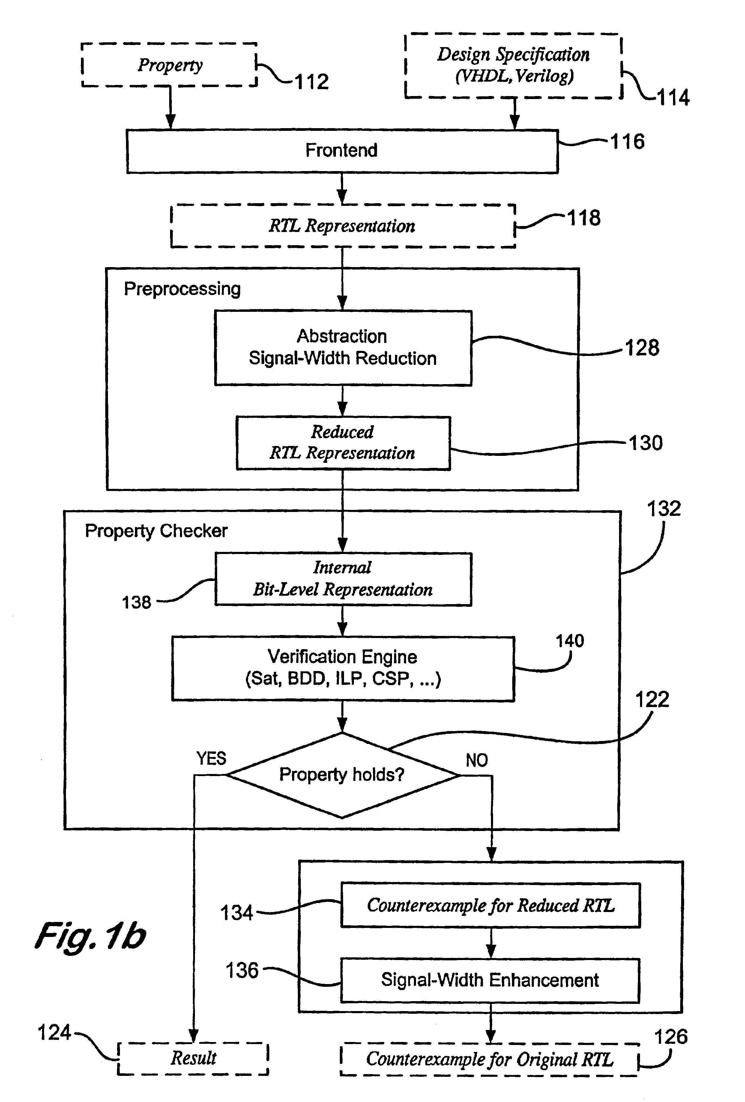
The invention may be understood more readily, and various other aspects and features of the invention may become apparent, from consideration of the following description and the figures as shown in the accompanying drawing sheets, wherein:
FIG. 2 shows the basic steps involved in the abstraction technique of this invention;
FIG. 3 is a table detailing the syntax of various bit-vector operators supported in the reduction technique of this invention;

Problems solved by technology

With designs continually increasing in size and complexity the test for correct behaviour becomes more important and a major economic issue, but at the same time becomes more complex, time consuming and expensive.
This problem has been widely investigated and continues to be so because efficient SAT techniques can greatly affect the operation of many EDA tools.
However a major limitation of this approach is that there is a corresponding exponential increase in memory requirement for the operating system and in run times of the verification tools.
However, since practical gate-level circuit descriptions can be quite large, dealing with substantially large CNF formulae results in unacceptable CPU run times. However, circuit designs are usually defined in terms of Register-Transfer-Level (RTL) specifications, for example, coded in hardware description languages (HDL's) like VHDL or Verilog.

Method used


Image

  • Method of circuit verification in digital design
  • Method of circuit verification in digital design
  • Method of circuit verification in digital design

Examples


example 10

Let x.sub.[8], y.sub.[16], z.sub.[16] be bitvector variables and assume that E contains the following equation:

x.sub.[8] =(y.sub.[16] and z.sub.[16])[15,8] (8)

Assume that granularity analysis and minimum width abstraction yield the following results:

C.sub.1 ={. . . , x.sub.[8] ,y.sub.[16] ,z.sub.[16] , . . . }; .phi.(C.sub.i)=2

C.sub.i+1 ={. . . , y.sub.[16] , z.sub.[16] , . . . }; .phi.(C.sub.i+1)=3

The granularity of y.sub.[16], for example, is given by:

{y.sub.[16] ,y.sub.[16] }, i.e. y.sub.[16] [15,8].sym.y.sub.[16] [7,0]

According to the minimum chunk widths, the corresponding reduced variable is assembled as follows:

{y'.sub.[5] (4,3), y'.sub.[5] }, i.e. y'.sub.[5] =y'.sub.[5] [4,3].sym.y'.sub.[5] [2,0]

Hence, the reduced equation of E', which corresponds to (8) of E is: ##EQU6##

Indices of extraction expressions are modified according to the new chunk widths.

Method 1 and method 2 yield that the original system E of bitvector equations is satisfiable if and only if the reduced system...


PUM


Abstract

The present invention relates to a method of circuit verification in digital design and in particular, relates to a method of register transfer level property checking to enable the same. Today's electrical circuit designs frequently contain up to several million transistors, and circuit designs need to be checked to ensure that circuits operate correctly. Formal methods for verification are becoming increasingly attractive since they confirm design behavior without exhausting simulating a design. A digital circuit design verification method, prior to a property checking process for each property of a non-reduced RTL model, determines a reduced RTL model which retains specific signal properties of a non-reduced RTL model which are to be checked. A linear signal width reduction causes an exponential reduction of the induced state space. Reducing state space sizes in general goes hand in hand with reduced verification runtimes, thus speeding up verification tasks.

Description

The present invention relates to a method of circuit verification in digital design and in particular relates to a method of register transfer level property checking to enable the same.Today's electrical circuit designs frequently contain up to several million transistors and circuit designs need to be checked to ensure that circuits operate correctly. Formal methods for verification are becoming increasingly attractive since they confirm design behaviour without exhaustively simulating a design. Over the past years, bounded model checking and bounded property checking have increased in significance in electronic design automation (EDA). When checking large industrial circuits, long run times, ranging between hours and several days, are quite common. With designs continually increasing in size and complexity the test for correct behaviour becomes more important and a major economic issue, but at the same time becomes more complex, time consuming and expensive. Automated abstraction...

Claims


Application Information

Patent Timeline
Patent Type & Authority Patents(United States)
IPC IPC(8): G06F17/50
CPCG06F17/504G06F30/3323
Inventor JOHANNSEN, PEER
Owner ONESPIN SOLUTIONS
Why Eureka
Try Eureka