

Wafer defect measuring method and apparatus
a defect and measuring method technology, applied in the direction of crystal growth process, semiconductor/solid-state device testing/measurement, instruments, etc., can solve the problem of inability to measure the depth and size of each individual surface layer defect, the relative dimensional factor cannot be determined, and the depth of a polished specular surface cannot be obtained
- Summary
- Abstract
- Description
- Claims
- Application Information
AI Technical Summary
Benefits of technology
Problems solved by technology
Method used
Image

Examples
example 1
Measuring the Depth of a Defect
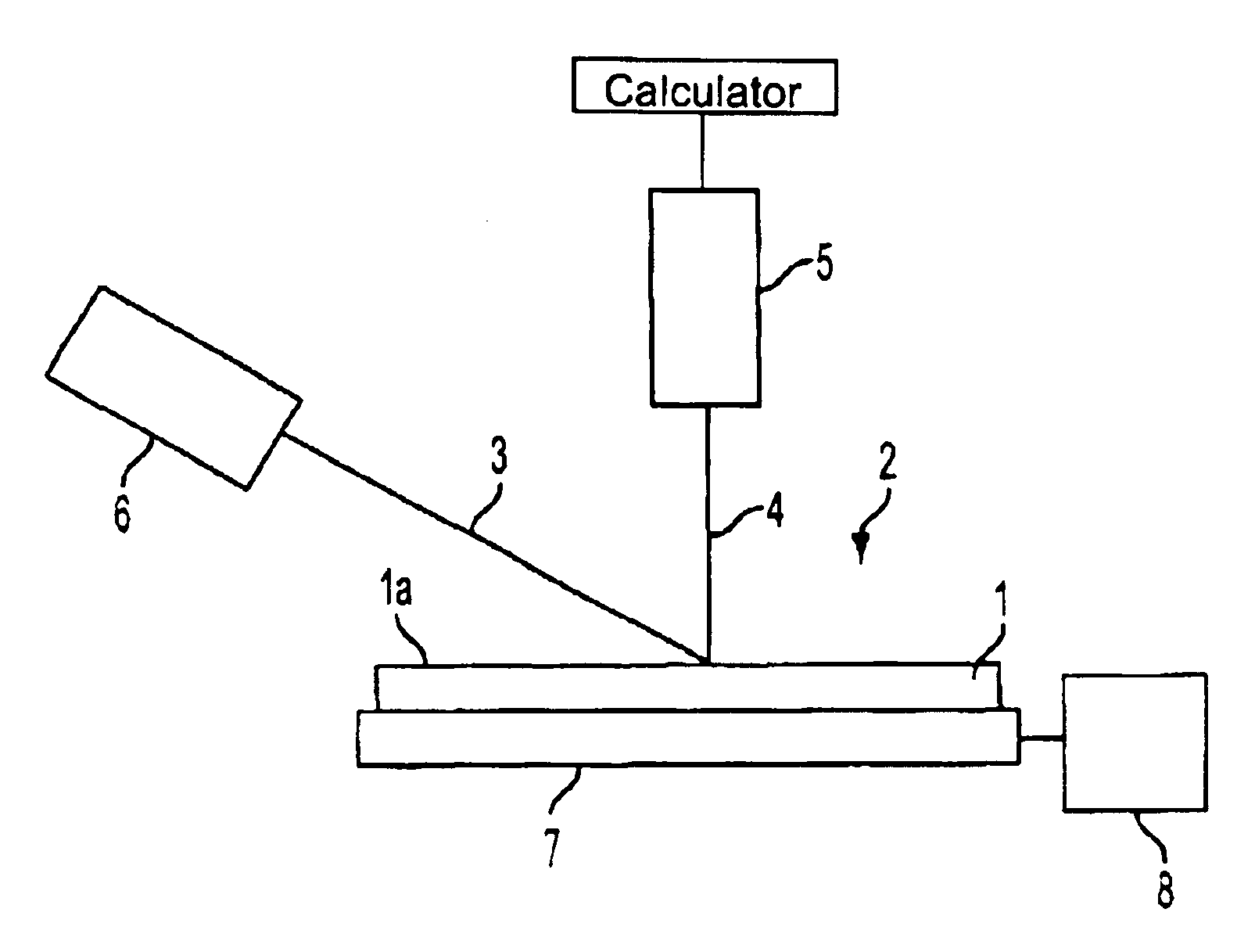
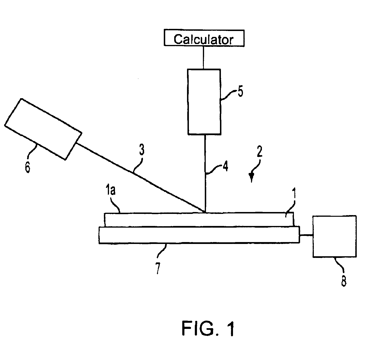
Using the apparatus shown in FIG. 1, a laser beam (about 1.8 eV) having a wavelength of 680 nm was applied to a polished specular surface of Si wafer (Si band gap: 1.12 eV) at an angle near Brewster angle (73.7.degree.) and the intensities of scattered beams from defects present in a wafer subsurface layer of a depth corresponding approximately to the penetration depth (about 3 .mu.m) of the laser beam were measured. Particularly, the intensities of scattered beams at Si wafer temperatures of 23.degree. C. and 83.degree. C. were measured.
In the measurement, the wafer temperature was controlled by means of a heater which was in contact with the wafer, and the wafer temperature was checked using a thermocouple.
As shown in FIG. 4, the scattered beam intensity, I.sub.23, of a certain defect at 23.degree. C. is measured and thereafter polishing is performed about .DELTA.d (cm) from the surface, followed by re-measurement of the scattered beam intensity, I.s...
example 2
Measuring a Relative Dimensional Factor
Using the apparatus shown in FIG. 1, a laser beam (about 1.8 eV) having a wavelength of 680 nm was applied to a polished specular surface of Si wafer (band gap of Si: 1.12 eV) at an angle near Brewster angle (73.7.degree.) and the intensity of a scattered beam generated from a defect present in a subsurface layer of the wafer corresponding to approximately the penetration depth (about 3 .mu.m) of the laser beam was measured. Particularly, scattered beam intensities at Si wafer temperatures of 23.degree. C. and 70.degree. C. were measured.
In the measurement, the wafer temperature was controlled with the heater disposed in contact with the wafer and was checked with a radiation thermometer. Absorption coefficient .alpha..sub.23 of Si for the laser beam of wavelength 680 nm at 23.degree. C. was 2322 cm.sup.-1 and that .alpha..sub.70 at 70.degree. C. was 2903 cm.sup.-1, with the difference being .DELTA..alpha.=.alpha..sub.70 -.alpha..sub.23 =581 cm...
example 3
Measuring the Number of Crystal Defects
Using the apparatus shown in FIG. 1, a laser beam (about 1.8 eV) having a wavelength of 680 nm was applied to a polished specular surface of Si wafer (Si band gap: 1.12 eV) at an angle near Brewster angle (73.7.degree.) and the intensity of a scattered beam from a defect present in a wafer subsurface layer of a depth corresponding approximately to the penetration depth of the laser beam was measured.
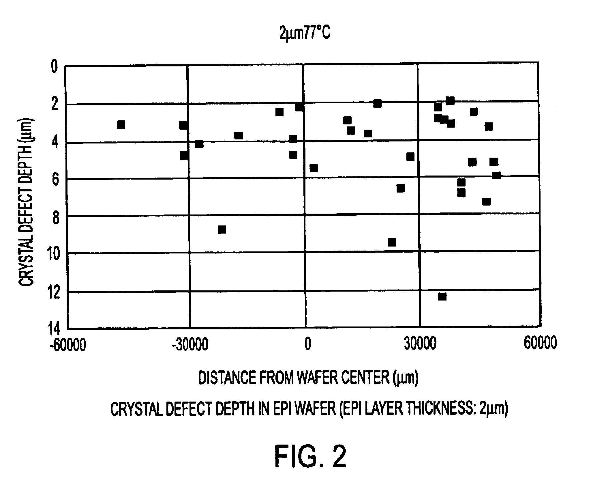
With reference to FIG. 5, a description will now be given of an experiment in which a change in the distribution of detected defects caused by a change in temperature was predicted. This prediction is for explaining the principle of the present invention in an easily understandable manner.
FIG. 5 shows in a comparative manner the distribution (indicated in white) of defects in crystal detected by a single wavelength, two-temperature type, laser scattering tomography of Si wafer at 23.degree. C. and 70.degree. C. and the distribution (indicated in bla...
PUM
 Abstract
Description
Claims
Application Information