Balancing planarization of layers and the effect of underlying structure on the metrology signal

a technology of balancing planarization and metrology signal, which is applied in the direction of optical radiation measurement, semiconductor/solid-state device testing/measurement, instruments, etc., can solve the problems of random and/or systematic noise of measured reflected optical signals, and achieve the effect of minimizing random and/or systematic noise and improving the planarization characteristics of layers

Inactive Publication Date: 2004-06-01
TOKYO ELECTRON US HOLDINGS INC
View PDF13 Cites 24 Cited by
  • Summary
  • Abstract
  • Description
  • Claims
  • Application Information

AI Technical Summary

Benefits of technology

The present invention is a method and system for identifying an underlying structure that achieves improved planarization characteristics of layers while minimizing introduction of random and / or systematic noise to the reflected metrology signal.

Problems solved by technology

The presence of a pattern in the underlying structure may introduce random and / or systematic noise to the measured reflected optical signal.
Significant random or systematic noise in the signal in turn skews the matching process of the measured reflected signal against the library of calculated reflected beam data, causing the match of the measured reflected signal to a different profile and / or different critical dimensions.

Method used


Image

  • Balancing planarization of layers and the effect of underlying structure on the metrology signal
  • Balancing planarization of layers and the effect of underlying structure on the metrology signal
  • Balancing planarization of layers and the effect of underlying structure on the metrology signal

Examples


Embodiment Construction

)

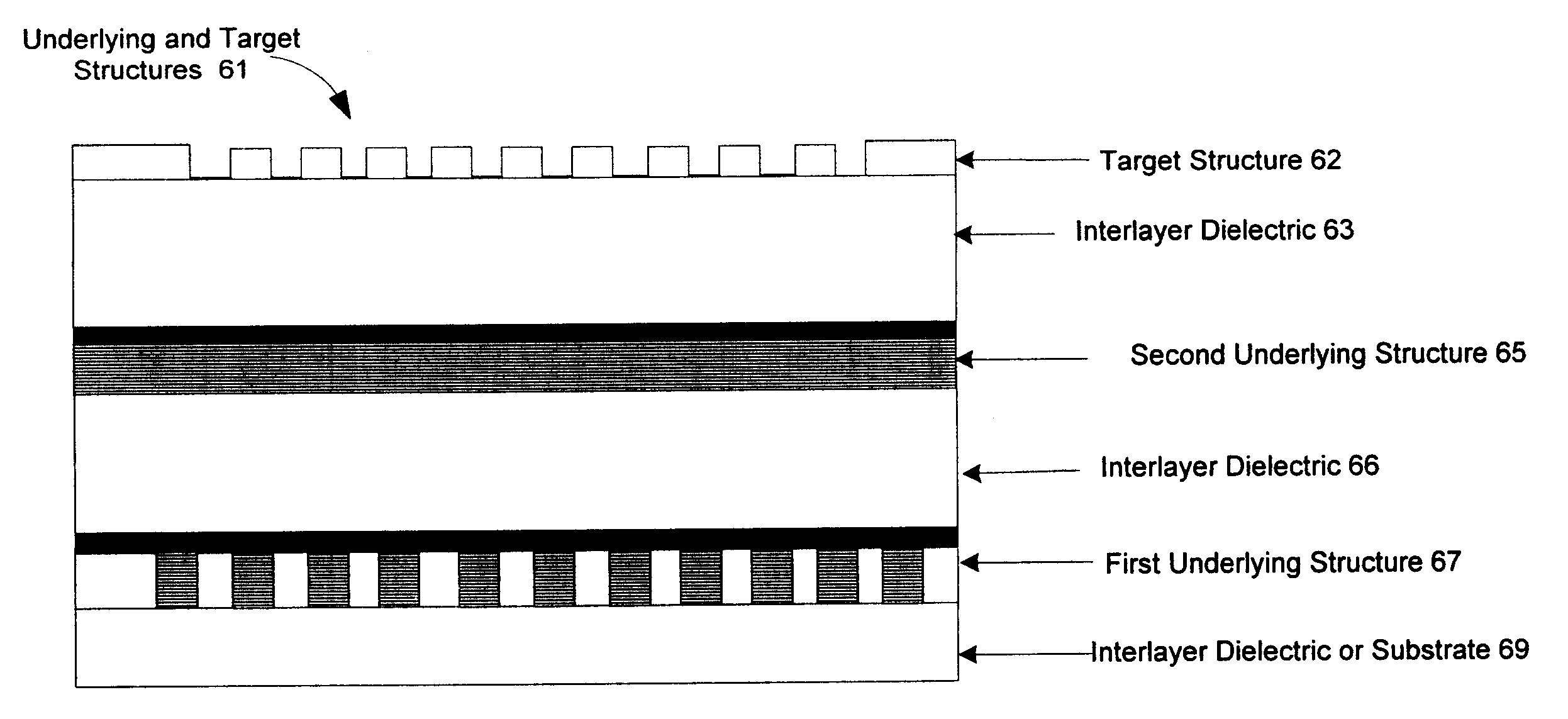
The present invention includes a method for identifying, for a given target structure, the design, distribution, and density of fill shapes of the underlying structures and / or the arrangement of the patterned underlying structures that will minimize the introduction of random or systematic noise to the reflected metrology signal off the target structure.

A summary of the process for the present invention, described in detail in FIG. 8, is provided here to facilitate the descriptions of figures that follow. Initially, the CMP and optical metrology signal design criteria for the target structure are set. A target structure is the patterned structure of a layer of a wafer that is measured using optical metrology. A predetermined set of underlying structures, including a calibration underlying structure, is designed. Based on the CMP design criteria, a set of pads and / or random shapes of varying size, geometry, and loading factors may be designed in a mask for the underlying structures....


PUM

PropertyMeasurementUnit
sizesaaaaaaaaaa
sizesaaaaaaaaaa
optical metrologyaaaaaaaaaa

Abstract

One embodiment of the present invention is a method of designing underlying structures in a wafer with pads of varying sizes and varying loading factors, and selecting the design of pads that yield a reflected metrology signal closest to the calibration metrology signal and that meet preset standard planarization characteristics. Another embodiment is a method of designing underlying structures with random shapes of varying sizes and varying loading factors. Still another embodiment is the use of periodic structures of varying line-to-space ratios in one or more underlying layers of a wafer, the periodicity of the underlying periodic structure being positioned at an angle relative to the direction of periodicity of the target periodic structure of the wafer.

Description

BACKGROUND OF INVENTION1. Field of InventionThis invention is in the field of manufacture of semiconductor devices. More particularly, this invention relates to a method and system of fabricating underlying structures to improve planarization characteristics of layers while minimizing introduction of random and / or systematic noise by the underlying structures to the metrology signal.2. Related ArtAs feature sizes in semiconductor devices shrink, photolithographic equipment requires that layers of a wafer be very flat or planar so that small feature dimensions are accurately patterned. Chemical mechanical planarization (CMP) is widely used in various semiconductor processing operations to planarize layers of a wafer. The polishing process typically uses an abrasive slurry and a combination of mechanical and chemical actions to planarize the layer surface.CMP performance is affected by the density of underlying structures in a wafer, resulting in two phenomena called "dishing" and "er...

Claims


Application Information

Patent Timeline
Patent Type & Authority Patents(United States)
IPC IPC(8): G01N21/47G01N21/956G01N21/88G01N21/95H01L23/58H01L21/3105
CPCG01N21/4788G01N21/9501G01N21/956H01L22/32H01L21/31053
Inventor JAKATDAR, NICKHILNIU, XINHUI
Owner TOKYO ELECTRON US HOLDINGS INC
Why Eureka
Try Eureka