Clock and data recovery circuit and clock control method thereof

a clock control and data recovery technology, applied in the direction of pulse manipulation, pulse technique, generating/distributing signals, etc., can solve the problems of data bits that cannot be sampled correctly, data of the correct value will no longer be able to be sampled,

Inactive Publication Date: 2004-06-22
RENESAS ELECTRONICS CORP
View PDF3 Cites 40 Cited by
  • Summary
  • Abstract
  • Description
  • Claims
  • Application Information

AI Technical Summary

Benefits of technology

Accordingly, it is an object of the present invention to provide a clock and data recovery circuit and method that make it possible to suppress the effects of jitter components and to sample data accurately.

Problems solved by technology

Hence, there is a greater possibility that data of the correct value will no longer be able to be sampled.
Thus, there are instances where the data bit cannot be sampled correctly.

Method used


Image

  • Clock and data recovery circuit and clock control method thereof
  • Clock and data recovery circuit and clock control method thereof
  • Clock and data recovery circuit and clock control method thereof

Examples


embodiments

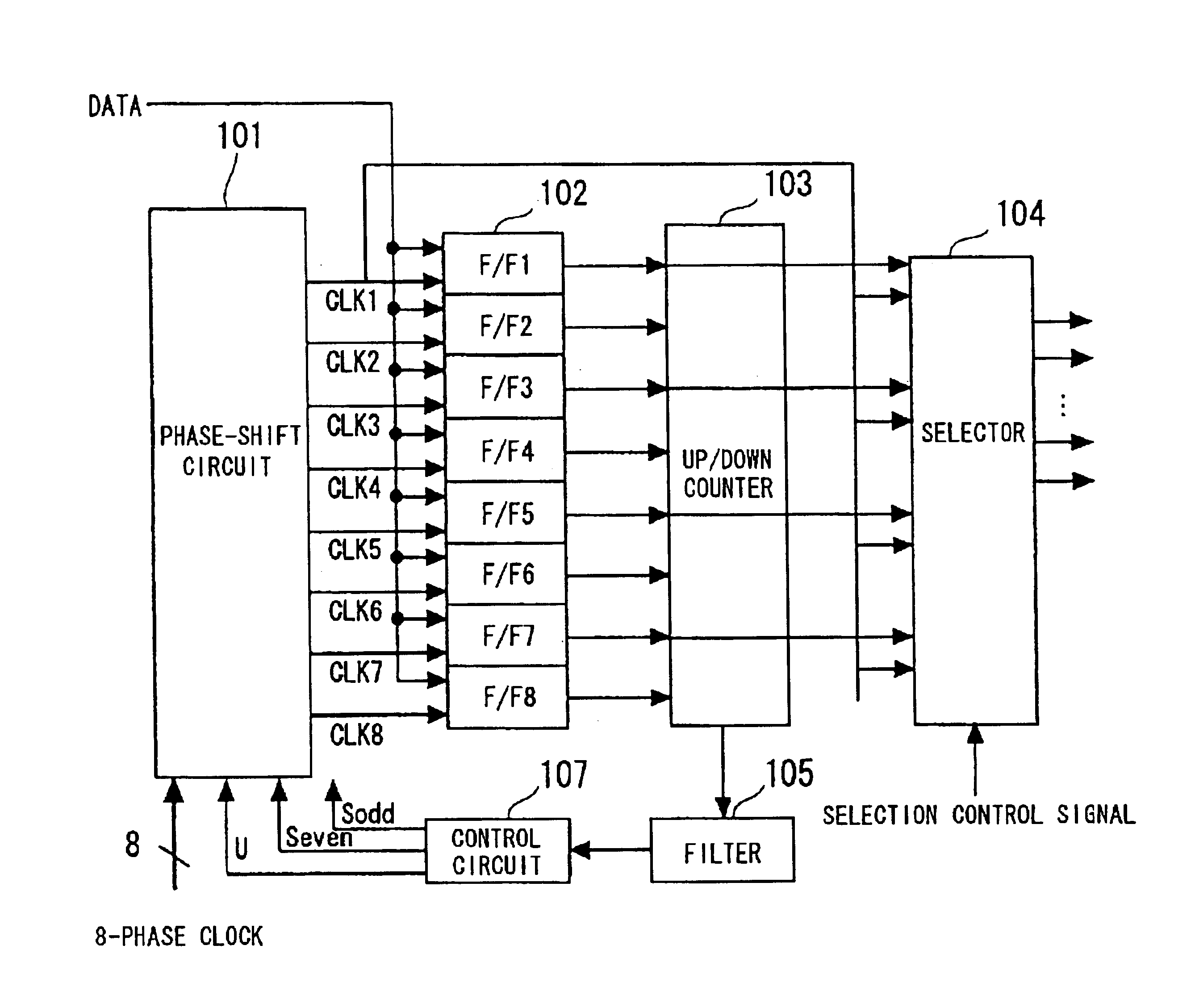
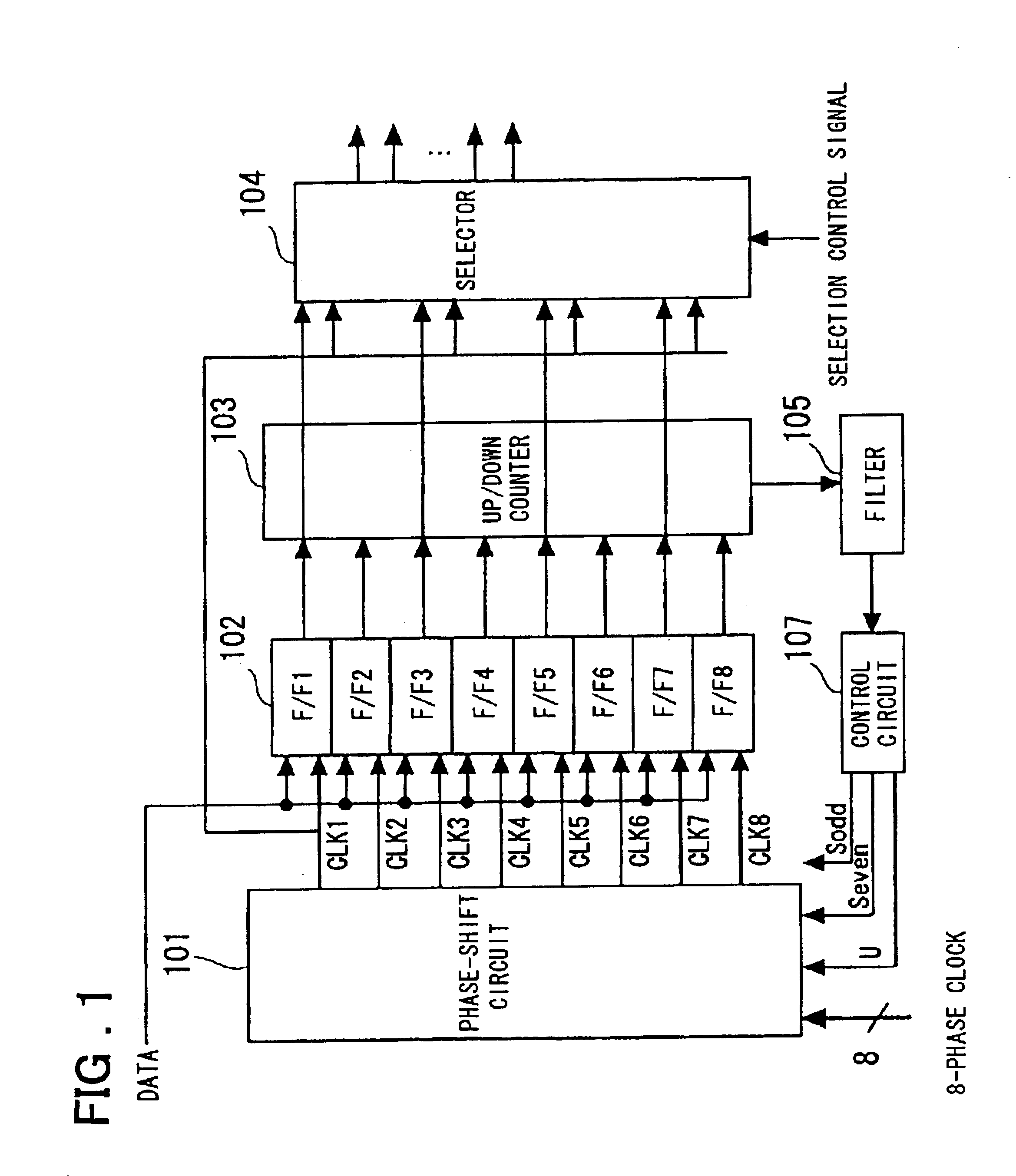
A preferred embodiment of the present invention will now be described in further detail with reference to the drawings. FIG. 1 is a diagram illustrating the structure of a preferred embodiment of the invention. As shown in FIG. 1, a clock and data recover circuit according to the present embodiment of the clock and data recovery circuit according to the invention comprises a phase-shift circuit 101, a plurality of D-type flip-flops 102 (F / F1 to F / F8), a counter 103, a selector 104, a filter, and control circuit 107.

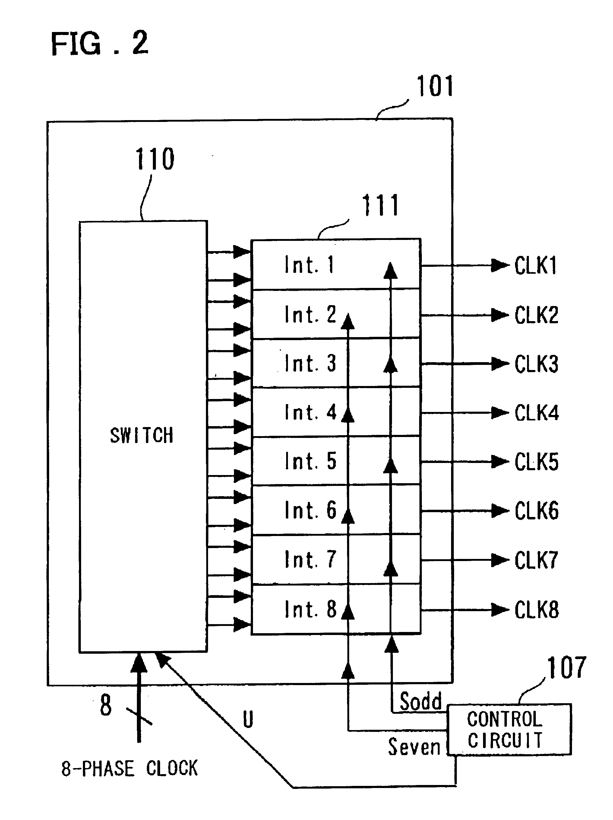
The phase-shift circuit 10 receives 8-phase clock signals, and outputs 8-sets of clock signals (CLK1-CLK8), which undergo phase shifting.

The D-type flip-flops 102 (F / F1 to F / F8) which have clock input terminals to which the clock signals output from the phase-shift circuit 101 are supplied, and data input terminals to which the input data DATA is supplied, sample the input data DATA at the rising edges of the clock signals.

The counter 103 counts up / down a count value resp...


PUM


Abstract

A clock and data recovery circuit includes a phase-shift circuit having a switch, which receives multiphase clocks, for selecting and outputting a plurality of clock pairs from among the multiphase clocks, and a plurality of interpolators, which receive the plurality of clock pairs output from the switch, for outputting clock signals in which delay time is stipulated by time obtained by performing interior division of the phase difference between the clocks of the pair; a plurality of latch circuits which receive input data in common; a phase detecting circuit for detecting and outputting phase, with respect to the clock, of a transition point of the input data from the outputs of the plurality of latch circuits; a filter for smoothing the output of the phase detecting circuit; and a control circuit for controlling clock phase by outputting control signals for controlling the interpolators and / or switch of the phase-shift circuit based upon the filter output.

Description

This invention relates to a clock and data recovery circuit and clock control method thereof.FIG. 8 is a diagram illustrating the structure of a clock and data recovery circuit according to the prior art. As shown in FIG. 8, the clock and data recovery circuit has a voltage-controlled oscillator (VCO) 51 of a PLL (phase Locked Loop) which generates a multiphase clock (multiphase output) of equally spaced phase differences from a reference clock (Ref CLK) applied thereto. The VCO comprises an analog ring oscillator, which is composed by an odd-number of inverter circuits connected into a ring-shaped configuration. A multiphase clock of equally spaced phase differences is extracted differentially from the outputs of differential inverting circuits constructing the ring oscillator. The clock and data recovery circuit has a plurality of flip-flops 52 (F / F1 to F / F8), which have data input terminals for receiving the input data DATA commonly and clock input terminals for receiving respect...

Claims


Application Information

Patent Timeline
Patent Type & Authority Patents(United States)
IPC IPC(8): H03K5/13H04L7/033H03K5/00G06F1/06G06F1/12H03K5/15H03L7/00H03L7/06H03L7/08H03L7/081H03L7/087H03L7/091H03L7/099H04L7/00H04L7/02
CPCH03K5/133H03L7/0814H03L7/087H03L7/091H04L7/0337H03K2005/00065H03K2005/00071H03K2005/00195H03L7/0998H04L7/0025
Inventor SAEKI, TAKANORI
Owner RENESAS ELECTRONICS CORP
Why Eureka
Try Eureka