

Liquid crystal panel
a liquid crystal display panel and matrix type technology, applied in the field of segmental and matrix type liquid crystal display panels, can solve the problems of the inability to control the display state in the other area (background area), and the inability to easily reverse the brightness and darkness of the display
- Summary
- Abstract
- Description
- Claims
- Application Information
AI Technical Summary
Benefits of technology
Problems solved by technology
Method used
Image

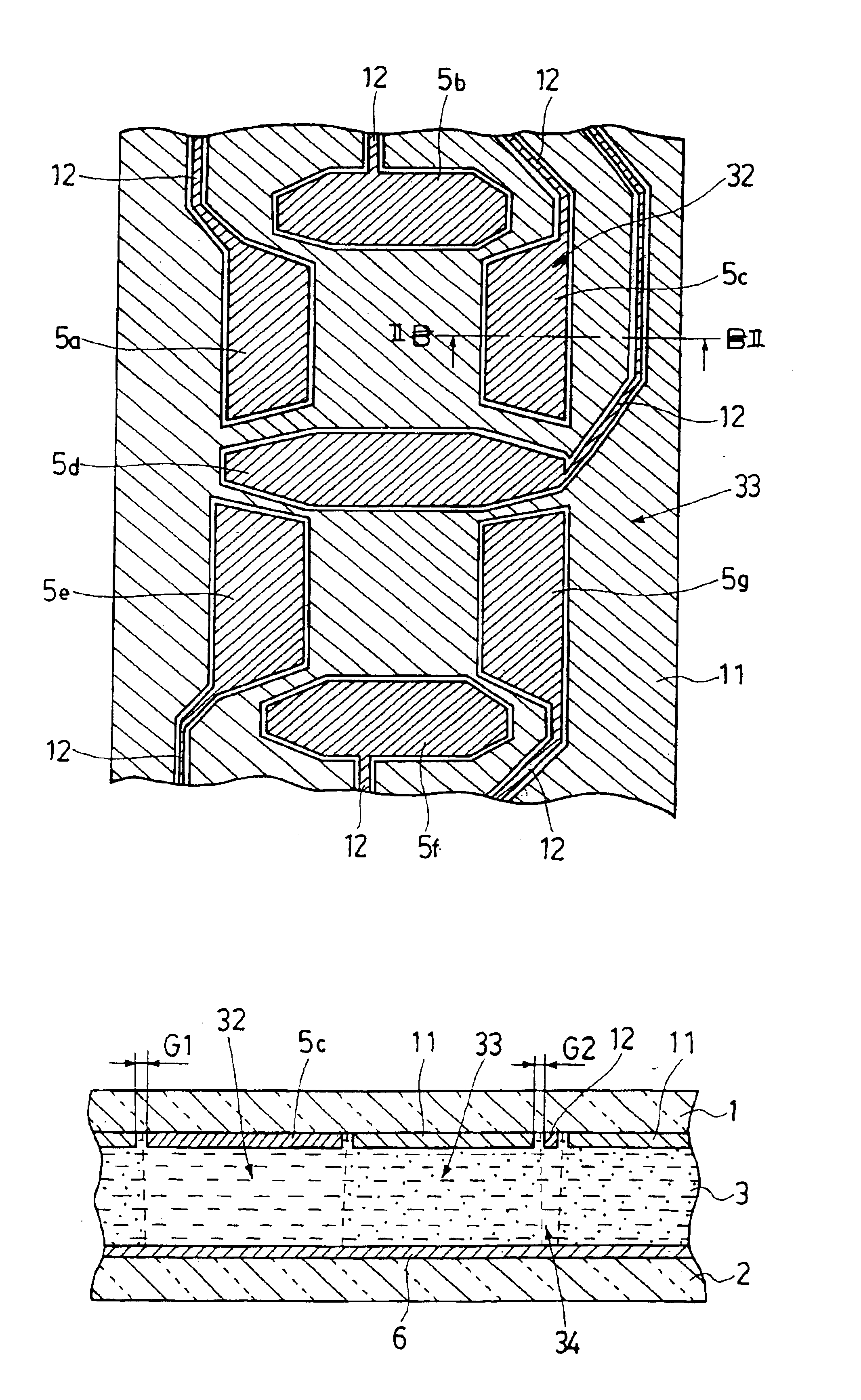
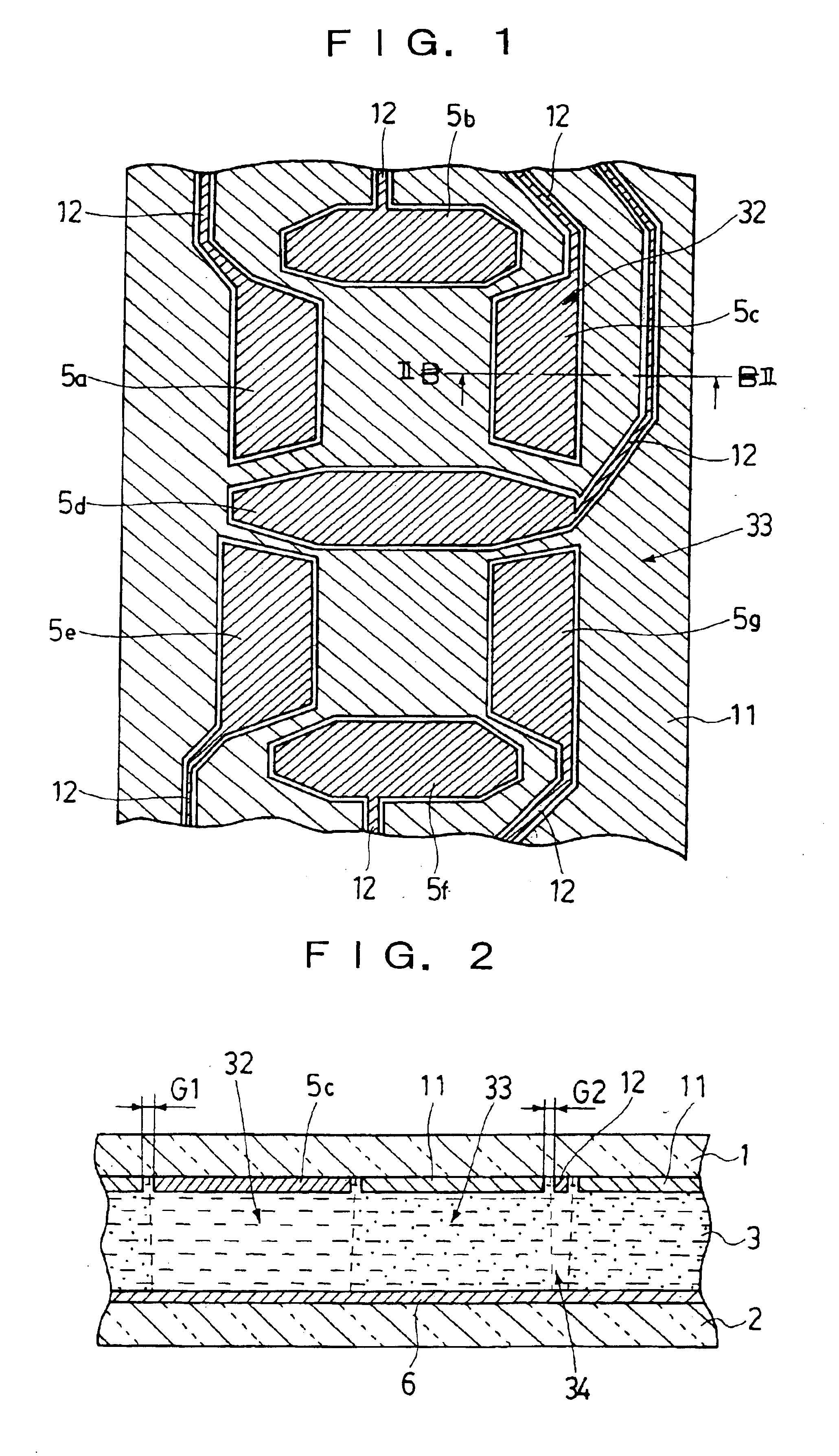
Examples
second embodiment
Next, the second embodiment of the liquid crystal display panel according to the invention is explained with FIG. 7 to FIG. 9.
FIG. 7 is a plane view showing a simplified arrangement example of the segment electrodes and the auxiliary electrode which are formed on the inner surface of the transparent upper substrate of the liquid crystal display panel, and FIG. 8 is a plane view showing an example of a split form of the opposite electrodes formed on the lower substrate. FIG. 9 is a perspective plane view of a state in which the upper substrate and the lower substrate are coupled together as viewed from above the upper substrate.
In these drawings, portions corresponding to those of the first embodiment shown in FIG. 1 to FIG. 3 are assigned the same numerals and symbols.
On the inner surface of the upper substrate (first substrate) 1 of the liquid crystal display panel, as shown in FIG. 7, a plurality of segment electrodes 5 made of an ITO film and thin wiring electrodes 12 integrated ...
third embodiment
Next, the third embodiment of the liquid crystal display panel according to the invention is explained with FIG. 10 to FIG. 14.
FIG. 10 is a rear view showing a part on the upper substrate side of the liquid crystal display panel, and FIG. 11 is a partially enlarged cross-sectional view corresponding to a cross section taken along a line XI--XI in FIG. 10 of the liquid crystal display panel. FIG. 12 is a rear view showing the state in which the auxiliary electrode is formed on the upper substrate, FIG. 13 is a rear view showing the state in which an insulating film is further formed on the upper substrate shown in FIG. 12, and FIG. 14 is a plane view showing a part on the lower substrate side of the liquid crystal display panel.
In these drawings, portions corresponding to those of the first embodiment shown in FIG. 1 to FIG. 3 are assigned the same numerals and symbols, and the description thereof is simplified.
In this liquid crystal display panel, the auxiliary electrode 11 made of ...
fourth embodiment
Next, the fourth embodiment of the liquid crystal display panel according to the invention is explained with FIG. 15 to FIG. 20.
FIG. 15 is a rear view showing a part on the upper substrate side of the liquid crystal display panel, and FIG. 16 is a partially enlarged cross-sectional view corresponding to a cross section taken along a line XVI--XVI in FIG. 15 of the liquid crystal display panel. FIG. 17 is a rear view showing a pattern of only the segment electrodes formed on the upper substrate, FIG. 18 is a rear view showing a pattern of only the insulating film formed on the upper substrate of the same, and FIG. 19 is a rear view showing a pattern of only the auxiliary electrode formed on the upper substrate of the same. FIG. 20 is a partially enlarged view of the wiring electrode formed integrally with the segment electrode.
In these drawings, portions corresponding to those of the first embodiment shown in FIG. 1 to FIG. 3 are assigned the same numerals and symbols, and the descri...
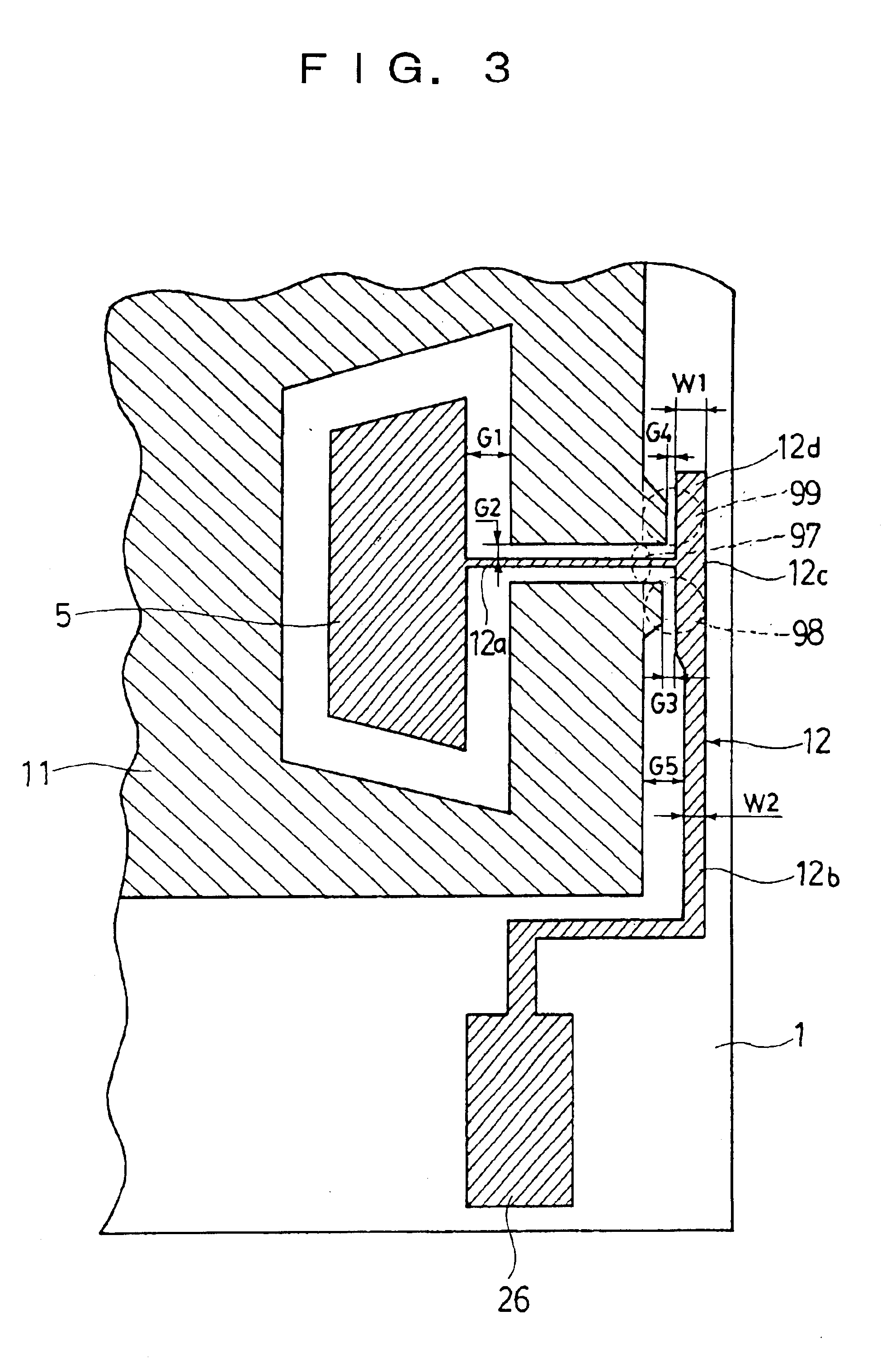
PUM
| Property | Measurement | Unit |
|---|---|---|
| width | aaaaa | aaaaa |
| thick | aaaaa | aaaaa |
| width W2 | aaaaa | aaaaa |
Abstract
Description
Claims
Application Information