Light emitting device and method of manufacturing the same

a technology of light emitting devices and manufacturing methods, applied in the field of semiconductor devices, can solve the problems of non-uniform surface potential distribution and higher film resistance of transparent electrodes, and achieve the effect of efficient diffusion of hydrogen and increased light emitting devices

Inactive Publication Date: 2004-08-24
SEMICON ENERGY LAB CO LTD
View PDF10 Cites 215 Cited by
  • Summary
  • Abstract
  • Description
  • Claims
  • Application Information

AI Technical Summary

Benefits of technology

If heat treatment is performed within a range of temperature to which the organic compound layer can be resistant and heat generated when the light emitting element emits the light is utilized, hydrogen can be diffused from the film containing hydrogen to terminate defects in the organic compound layer with hydrogen (termination). By terminating the defects in the organic compound layer with hydrogen, the light emitting device can be increased in its reliability. Also, when the film containing hydrogen is formed, hydrogen turned into a plasma can be used to terminate defects in the organic compound layer with hydrogen. The protective film formed so as to cover the film containing hydrogen also functions to block hydrogen diffused toward the protective film side and to efficiently diffuse hydrogen into the organic compound layer to terminate defects in the organic compound layer with hydrogen. Further, the film containing hydrogen can serve as the protective film for the light emitting element.
Further, the film containing hydrogen can serve as a buffer layer. When the silicon nitride film is formed in contact with the transparent conductive film by a sputtering method, there is a possibility that impurities (In, Sn, Zn, etc.) contained in the transparent conductive film are mixed into the silicon nitride film. However, by forming the film containing hydrogen as a buffer layer therebetween, it is also possible to prevent mixture of the impurities into the silicon nitride film. According to the above structure, the buffer layer is formed, so that the impurities (In, Sn, etc.) can be prevented from mixing therein from the transparent conductive film and a superior protective film having no impurities can be formed.

Problems solved by technology

In the above-mentioned respective structures, there arises a problem concerning a higher film resistance of a transparent electrode.
If the film resistance of the transparent electrode serving as an anode or a cathode is increased, there arises a problem in that a potential distribution in the surface becomes nonuniform due to voltage drop, which involves variations in luminance of the light emitting element.

Method used


Image

  • Light emitting device and method of manufacturing the same
  • Light emitting device and method of manufacturing the same
  • Light emitting device and method of manufacturing the same

Examples


embodiment mode 1

[Embodiment Mode 1]

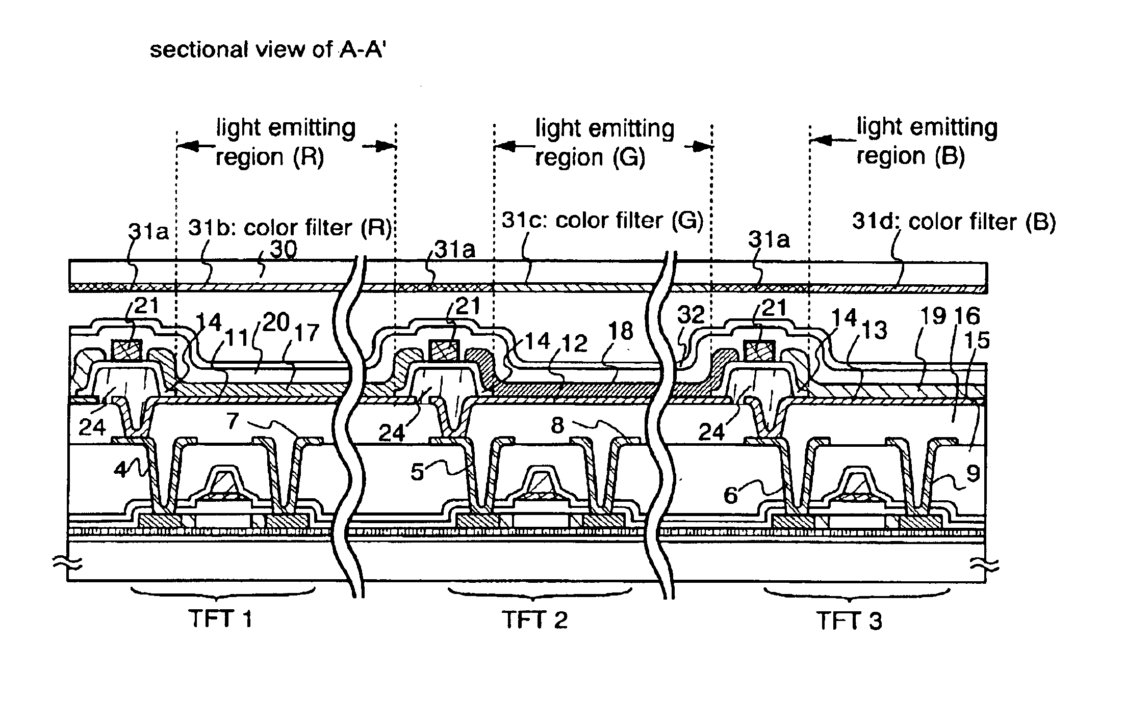
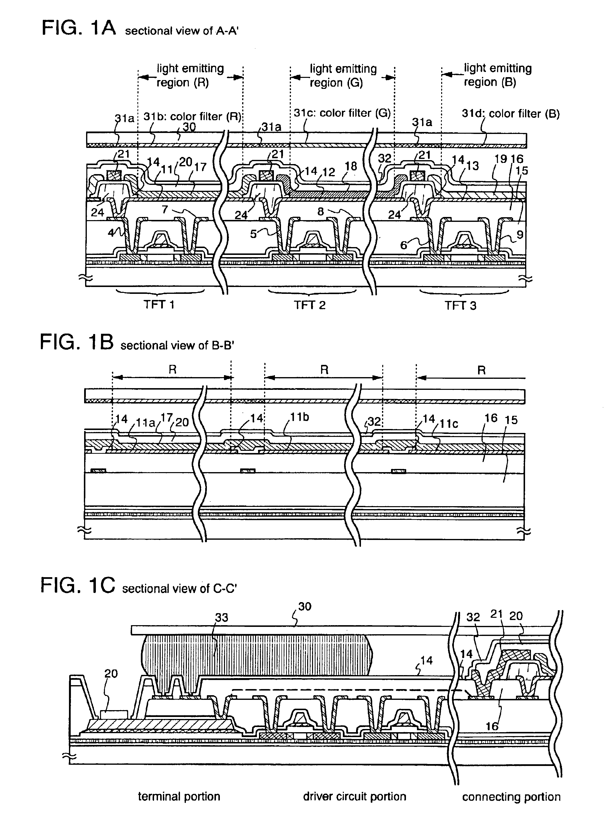
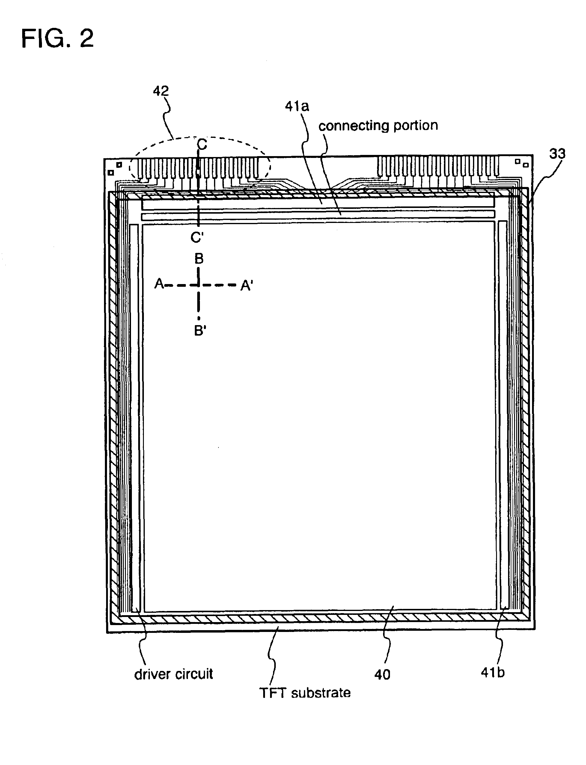
FIG. 2 is a top view of an EL module. In the figure, over a substrate (also referred to as TFT substrate) where a number of TFTs are provided, there are formed a pixel portion 40 used for display, driver circuits 41a and 41b for driving pixels of the pixel portion, a connecting portion for connecting an electrode formed on an EL layer and a lead wiring, and a terminal portion 42 to which an FPC is attached for connecting an external circuit therewith. Also, a substrate for sealing an EL element and a sealing member 33 are used to attain a sealed state. FIG. 1A is a sectional view taken along the dashed line A-A' of FIG. 2.

The pixels are arranged regularly in the direction of the dashed line A-A'. Here, an example of the pixels arranged in the order of R, G, and B in an X direction will be shown.

In FIG. 1A, a light emitting region (R) indicates a region for emitting a red light; a light emitting region (G), a region for emitting a green light; and a light emitting ...

embodiment mode 2

[Embodiment Mode 2]

Here, the film containing hydrogen and the protective film will be described with reference to FIGS. 4A and 4B.

FIG. 4A is a schematic diagram showing an example of a laminate structure of the EL element. In FIG. 4A, reference numeral 200 denotes a cathode (or an anode); 201, an EL layer; 202, an anode (or a cathode); 203, a DLC film containing hydrogen; and 204, a protective film. When the emitted light is caused to pass through the anode 202, a conductive film having a light-transmissive property (ITO, ZnO, etc.) is preferably used as the anode 202. Also, as the cathode 200, a metal film (an alloy film of MgAg, MgIn, AlLi, etc. or a film formed by coevaporation of aluminum and an element belonging to Group 1 or 2 in the periodic table) or a laminate thereof is preferably used.

The protective film 204 may be made of an insulating film mainly containing silicon nitride or silicon oxynitride which is obtained by a sputtering method (DC system or RF system). The silic...

embodiment mode 3

[Embodiment Mode 3]

Here, FIGS. 6A to 6C show an example of a structure partially different from FIGS. 1A to 1C. In this example, among a number of pixels arranged regularly in the pixel portion, pixels in a 3.times.3 matrix are used by way of example and the present invention will be described below. Note that, in a sectional structure, TFTs of FIGS. 6A to 6C are substantially the same as those of FIGS. 1A to 1C and thus components identical to those of FIGS. 1A to 1C are denoted by identical reference numerals for simplicity.

FIG. 6A is a sectional view taken along the alternate long and short dash line A-A' of FIG. 5A. A light emitting region 50R indicates a red light emitting region; a light emitting region 50G, a green light emitting region; and a light emitting region 50B, a blue light emitting region. These light emitting regions of three colors realize a light emitting display device capable of full color display.

As shown in FIG. 6A, this embodiment mode employs an example in ...


PUM


Abstract

To provide a light emitting device high in reliability with a pixel portion having high definition with a large screen. According to a light emitting device of the present invention, on an insulator (24) provided between pixel electrodes, an auxiliary electrode (21) made of a metal film is formed, whereby a conductive layer (20) made of a transparent conductive film in contact with the auxiliary electrode can be made low in resistance and thin. Also, the auxiliary electrode (21) is used to achieve connection with an electrode on a lower layer, whereby the electrode can be led out with the transparent conductive film formed on an EL layer. Further, a protective film (32) made of a film containing hydrogen and a silicon nitride film which are laminated is formed, whereby high reliability can be achieved.

Description

BACKGROUND OF THE INVENTION1. Field of the InventionThe present invention relates to a semiconductor device and, particularly, to a light emitting device having an organic light emitting element formed over a substrate having an insulating surface and a manufacturing method therefor. The present invention also relates to a module in which an IC etc. including a controller is mounted on a panel having the organic light emitting element. Note that, in this specification, the panel and the module which have the organic light emitting element are collectively referred to as a light emitting device. Further, the present invention relates to an apparatus for manufacturing the light emitting device.Note that, in this specification, the term semiconductor device refers to the devices in general which can function by utilizing semiconductor characteristics. The light emitting device, an electro-optic device, a semiconductor circuit, and an electronic device are all included in the category o...

Claims


Application Information

Patent Timeline
Patent Type & Authority Patents(United States)
IPC IPC(8): H01L27/32H01L51/50H01L27/28H01L51/52
CPCH01L27/322H01L27/3246H01L51/5212H01L27/3272H01L27/3279H01L51/5228H01L27/3211H01L51/5253H01L2251/5315Y10S257/929H10K59/35H10K59/38H10K59/1315H10K59/122H10K50/814H10K50/824H10K50/844H10K2102/3026H05B33/00H10K59/123H10K59/126H10K59/131H10K59/352
Inventor YAMAZAKI, SHUNPEIHIROKI, MASAAKIMURAKAMI, MASAKAZUKUWABARA, HIDEAKI
Owner SEMICON ENERGY LAB CO LTD
Why Eureka
Try Eureka