

Light-emitting semiconductor potting composition and light-emitting semiconductor device
a technology of semiconductor potting and semiconductor devices, which is applied in semiconductor devices, semiconductor/solid-state device details, solid-state devices, etc., can solve the problems of poor durability to light, poor durability to moisture, and epoxy resins
- Summary
- Abstract
- Description
- Claims
- Application Information
AI Technical Summary
Benefits of technology
Problems solved by technology
Method used
Image

Examples
example 1
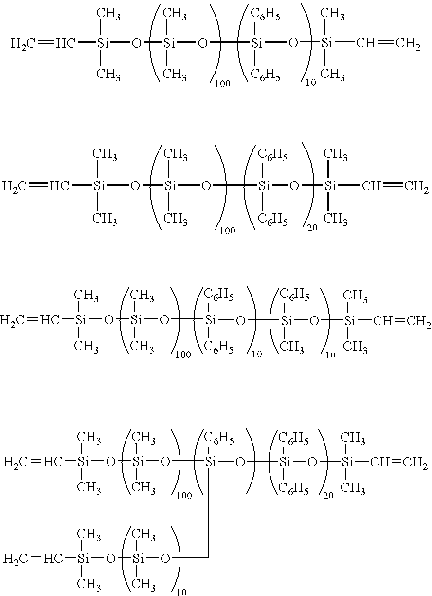
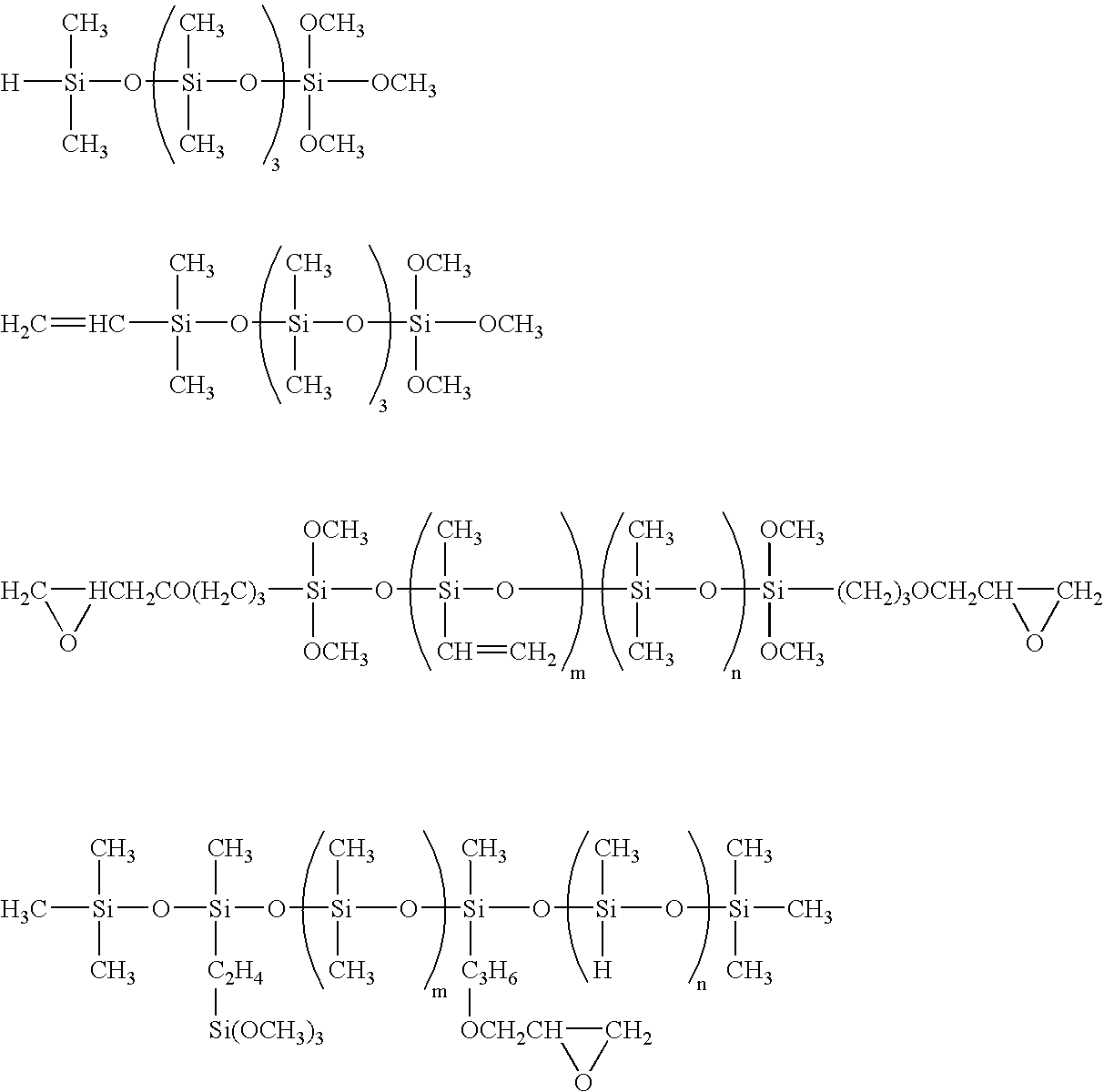
A silicone potting material was prepared by intimately mixing 100 parts of a vinyl-terminated dimethyldiphenylpolysiloxane (viscosity 3 Pa.s) having formula (I), 2.5 parts of a methylhydrogenpolysiloxane (viscosity 15 mPa.s) having formula (II), 0.03 part of 2-ethylhexyl alcohol-modified chloroplatinic acid solution (Pt concentration 2 wt %), 0.05 part of ethynylcyclohexyl alcohol, and 2 parts of an alkoxy-containing silicone compound having formula (III). ##STR6## ##STR7##
The potting material cured into a silicone resin which had a Durometer type A hardness of 33 and a refractive index of 1.48 at 25.degree. C. and 589 nm. Using the potting material, a light-emitting semiconductor device was fabricated as above.
example 2
A silicone potting material was prepared by intimately mixing 100 parts of a vinyl-terminated dimethyldiphenylpolysiloxane (viscosity 5 Pa.s) having formula (IV), 7.0 parts of a methylhydrogenpolysiloxane (viscosity 90 mPa.s) having formula (V), 0.03 part of 2-ethylhexyl alcohol-modified chloroplatinic acid solution (Pt concentration 2 wt %), 0.05 part of ethynylcyclohexyl alcohol, and 3 parts of 3-methacryloxypropyltrimethoxysilane. ##STR8##
The potting material cured into a silicone resin which had a Durometer type A hardness of 24 and a refractive index of 1.45 at 25.degree. C. and 589 nm. Using the potting material, a light-emitting semiconductor device was fabricated as above.
example 3
A silicone potting material was prepared by intimately mixing 100 parts of a vinyl-terminated dimethyldiphenylpolysiloxane (viscosity 2 Pa.s) having formula (VI), 4.1 parts of a phenylmethylhydrogenpolysiloxane (viscosity 30 mPa.s) having formula (VII), 0.03 part of 2-ethylhexyl alcohol-modified chloroplatinic acid solution (Pt concentration 2 wt %), 0.05 part of ethynylcyclohexyl alcohol, and 2 parts of an alkoxy-containing silicone compound having formula (VIII). ##STR9##
The potting material cured into a silicone resin which had a Durometer type A hardness of 62 and a refractive index of 1.53 at 25.degree. C. and 589 nm. Using the potting material, a light-emitting semiconductor device was fabricated as above.
PUM
| Property | Measurement | Unit |
|---|---|---|
| refractive index | aaaaa | aaaaa |
| refractive index | aaaaa | aaaaa |
| mol % | aaaaa | aaaaa |
Abstract
Description
Claims
Application Information