Photon detection enhancement of superconducting hot-electron photodetectors

Inactive Publication Date: 2004-12-07
ADVANCED MICRO DEVICES INC
View PDF6 Cites 9 Cited by
  • Summary
  • Abstract
  • Description
  • Claims
  • Application Information

AI Technical Summary

Problems solved by technology

Unfortunately, a typical conventional MCP-PMT detector has low quantum efficiency, especially in the near infrared region.
In particular, the detector loses virtually all sensitivity for wavelengths above 900 nm.
For acquisition of photon emission from the backside of silicon substrates, this has proved problematic.
This can lead to lengthy acquisition times.
Conventional SHEPs can exhibit a limited quantum efficiency.
The fallout of limited quantum efficiency is the possibility of the SHEP not detecting certain circuit switching events.
This may entail long testing periods.

Method used


Image

  • Photon detection enhancement of superconducting hot-electron photodetectors
  • Photon detection enhancement of superconducting hot-electron photodetectors
  • Photon detection enhancement of superconducting hot-electron photodetectors

Examples


Embodiment Construction

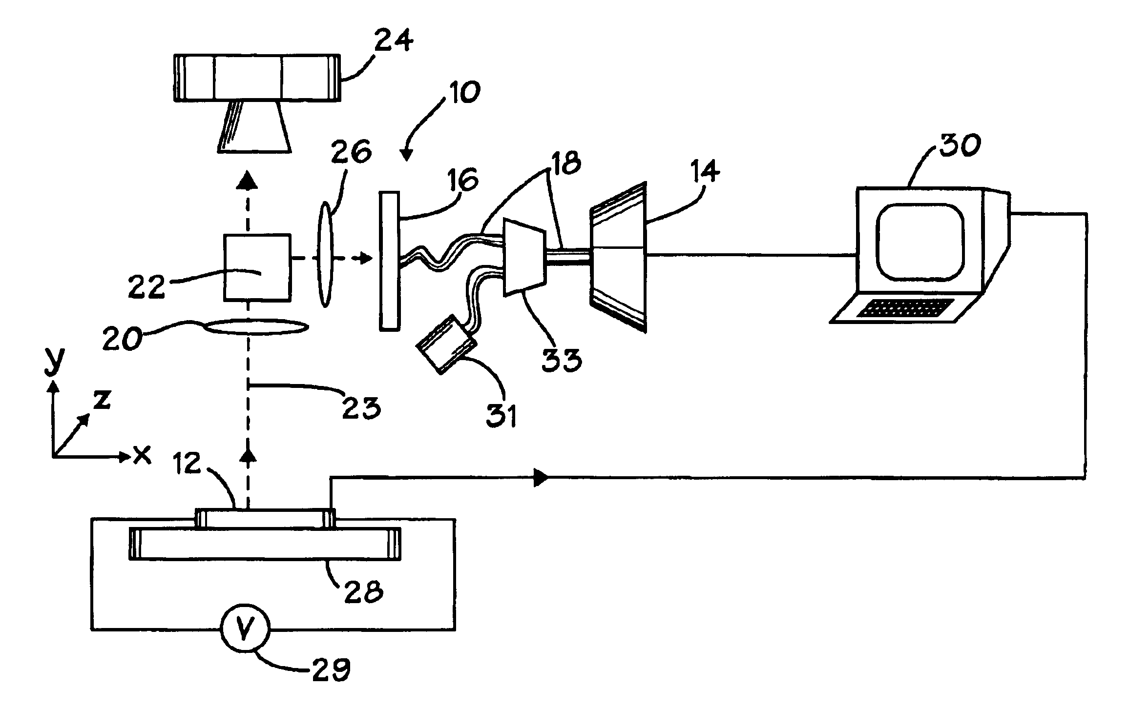
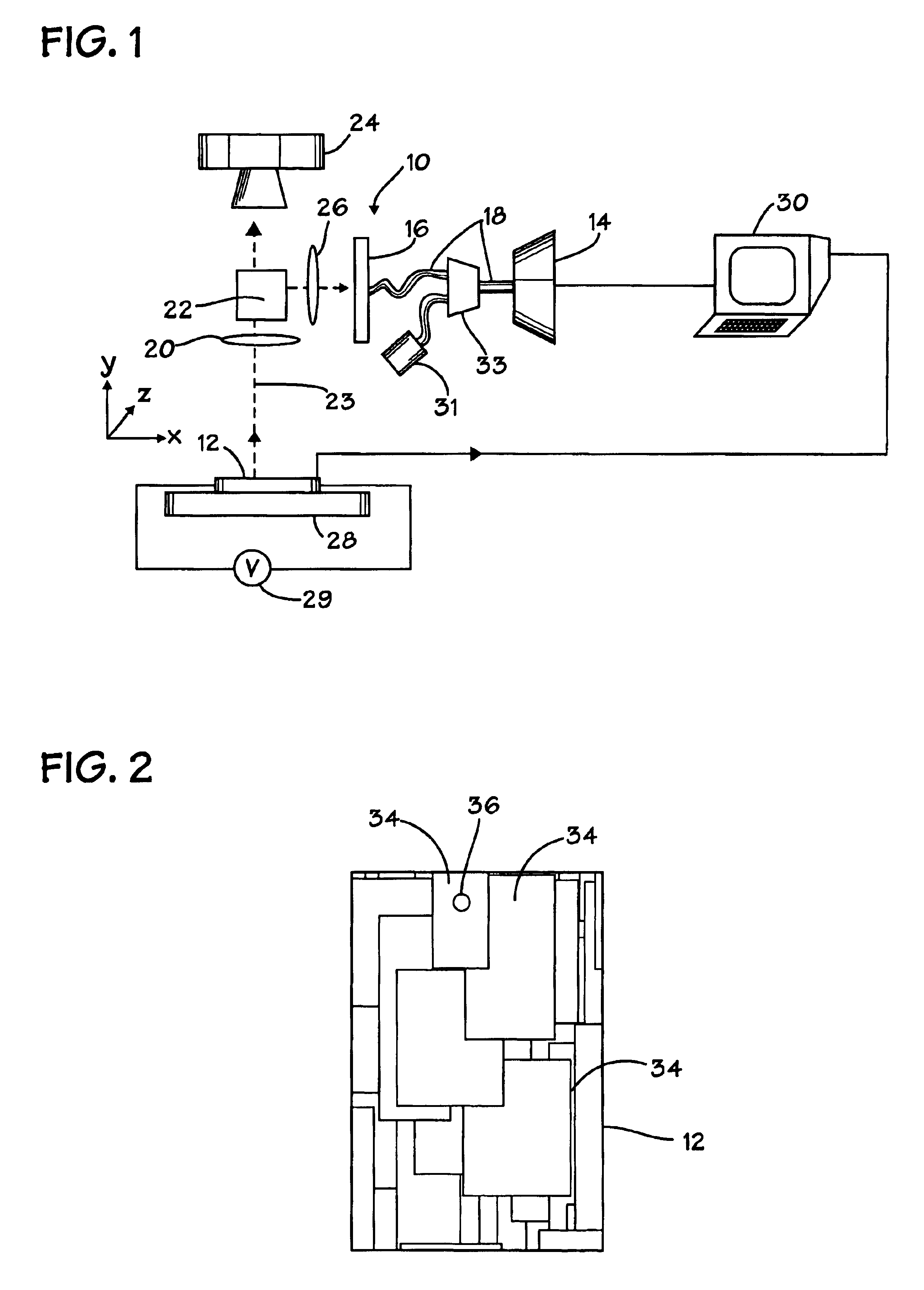
In the drawings described below, reference numerals are generally repeated where identical elements appear in more than one figure. Turning now to the drawings, and in particular to FIG. 1, therein is shown a schematic view of an exemplary imaging system 10 suitable for obtaining hot electron photon images of a workpiece 12. The workpiece 12 may be a semiconductor wafer, a semiconductor-on-insulator wafer or virtually any other type of substrate useful for circuit fabrication.

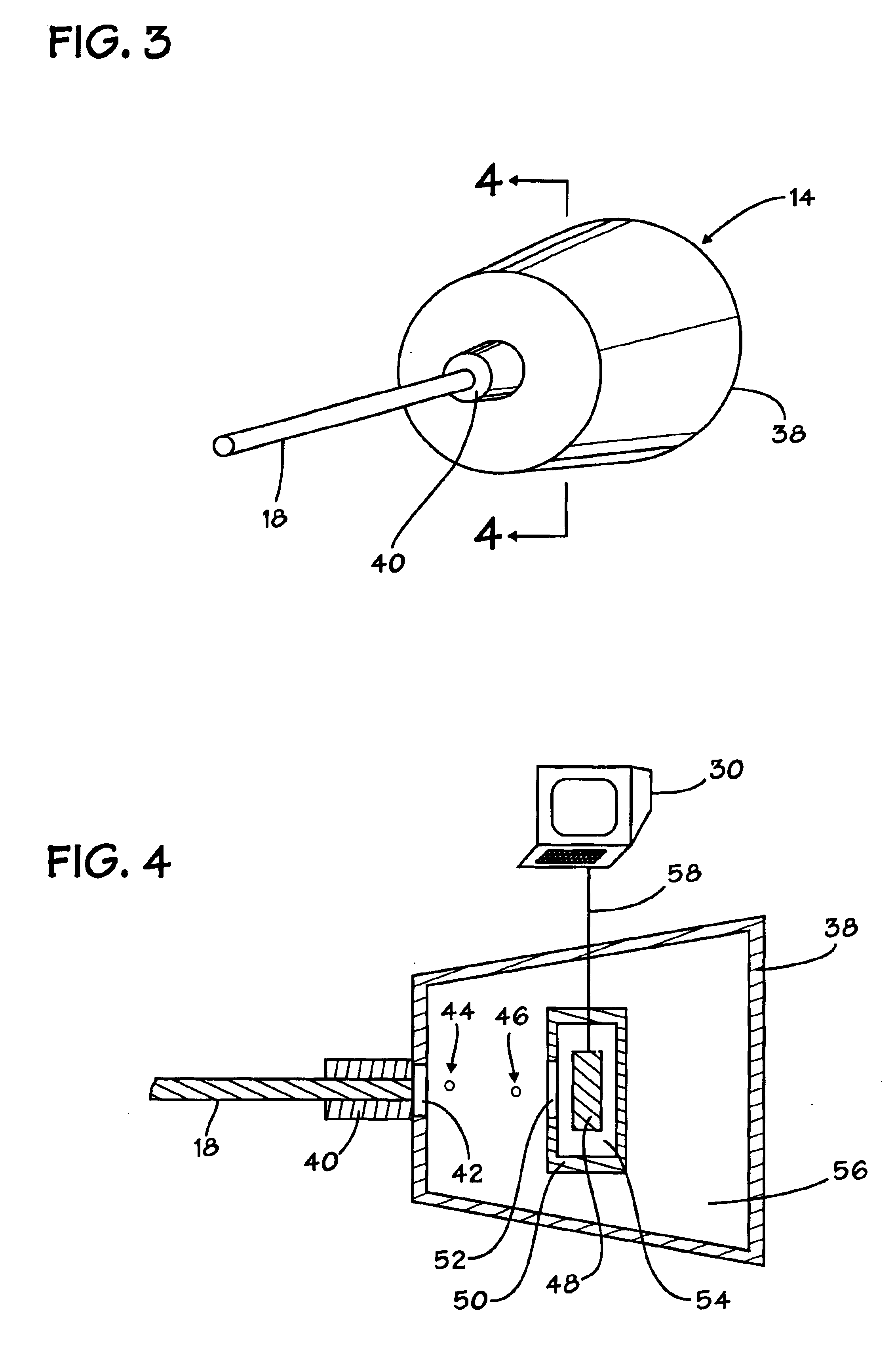
The system 10 utilizes a superconducting hot-electron photodetector ("SHEP) 14 that is linked to an aperture 16 by a fiber optic cable 18. The SHEP 14 is advantageously operated in a superconducting state. Impacting photons cause the superconducting state to change to a non-superconducting state which is sensed as a sudden change in the resistivity of the SHEP 14. The dark count rate of the SHEP 14 may be less than about 10.0 counts per second.

The aperture 16 is placed in a back imaging plane of an objective le...


PUM


Abstract

Various methods of hot-electron imaging a workpiece are provided. In one aspect, a method of examining a workpiece is provided that includes directing a first photon at a photodetector at a first known time and stimulating a circuit device of the workpiece at a second known time to produce a condition in the circuit device conducive to photon emission. At least one photon emitted by the circuit device in response to the stimulation is detected. The first photon increases the quantum efficiency of the photodetector in detecting the at least one photon. The detection of the at least one photon relative to the first known time and the second known time is time correlated to temporally distinguish the first photon and the at least one photon and to temporally correlate the stimulation of the circuit device to the detection of the at least one photon.

Description

1. Field of the InventionThis invention relates generally to semiconductor processing, and more particularly to methods of probing a workpiece using hot-electron induced photon emission.2. Description of the Related ArtFault-isolation techniques are critical to the development and manufacture of large-scale integrated circuits such as microprocessors. As the numbers of devices per integrated circuit have continued to climb and the sizes of those devices continued to shrink, methods have been developed to probe the operation of integrated circuits at the device level.Electron beam micro probing has been used for a number of years as a means of analyzing electrical wave forms generated by the various microscopic circuit structures in an integrated circuit. An electron beam ("e-beam") micro probe is a particularized type of electron microscope that is designed to provide a visual image of the circuit structures on an integrated circuit. E-beams are specifically focused at targeted circ...

Claims


Application Information

Patent Timeline
IPC IPC(8): G01R31/28G01R31/308
CPCG01R31/308
Inventor BRUCE, MICHAEL R.POWELL, ROBERTDAVIS, BRENNANGORUGANTHU, RAMACHU, THOMASSANTANA, JR., MIGUEL
Owner ADVANCED MICRO DEVICES INC
Why Eureka
Try Eureka