Dim-out method for organic EL panel

a technology of organic el panel and dimming method, which is applied in the direction of discharge tube luminescnet screen, static indicating device, instruments, etc., can solve the problems of deteriorating quality in the anode, damage to the cathode and further effects of other pixels, and ablation or other damage, so as to achieve the effect of dimming out a defective pixel

Inactive Publication Date: 2004-12-07
SANYO ELECTRIC CO LTD
View PDF2 Cites 13 Cited by
  • Summary
  • Abstract
  • Description
  • Claims
  • Application Information

AI Technical Summary

Benefits of technology

The present invention relates to a dim-out method used in an organic EL panel for effectively dimming out a defective pixel.
According to the present invention, a dim-out process can be performed by irradiating a laser beam on a semiconductor layer of the defective pixel. More specifically, in this process, crystal structure of the semiconductor layer is destructed at a micro level to increase resistance, there by executing electrical disconnection. In this manner, a favorable dim-out process that achieves dimming out of defective pixels basically without damaging other components can be performed.

Problems solved by technology

Even if it is only one pixel, one light-emitting point among surrounding dark or black pixels is noticeable to a viewer and is therefore regarded as a fault.
However, when a deactivation process using a visible light YAG laser is executed, there may result damages in the cathode and further effects on display by other pixels.
Accordingly, when a any of the TFT wiring is disconnected using a visible light YAG laser, the laser beam penetrates the cathode and often causes ablation or other damage.
The ablation may further cause quality in the anode to deteriorate, which may lead to undesirable influence on display by the surrounding pixels.
Degradation of the organic layer due to penetration of moisture, oxygen, or the like in the exposed portion can result in further defective pixels.
Moreover, when wiring is disconnected by ablation, the once scattered wiring material (typically metal) may attach to other wiring components and generate a short circuit.

Method used


Image

  • Dim-out method for organic EL panel
  • Dim-out method for organic EL panel
  • Dim-out method for organic EL panel

Examples


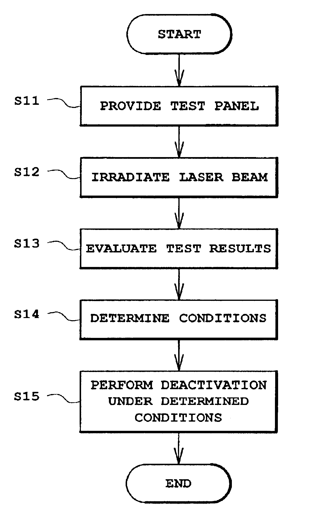
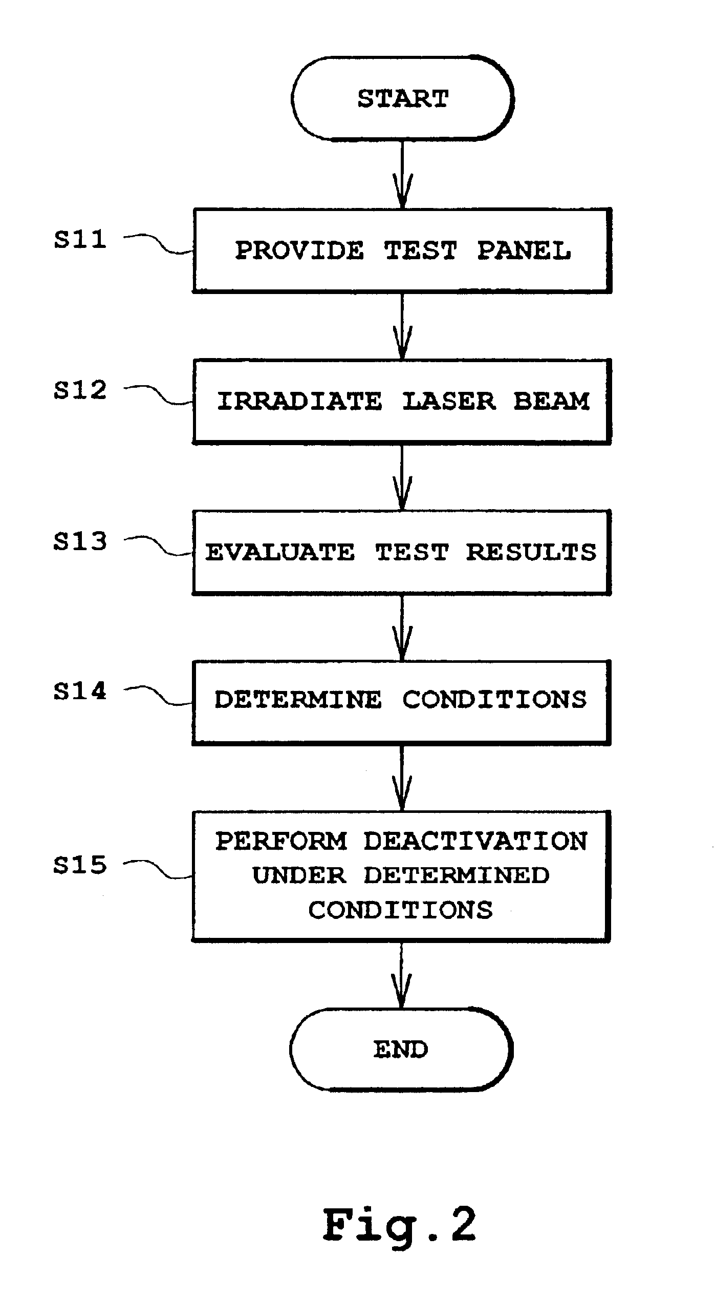
Embodiment Construction

A preferred embodiment of the present invention will now be described with reference to the accompanying drawings.

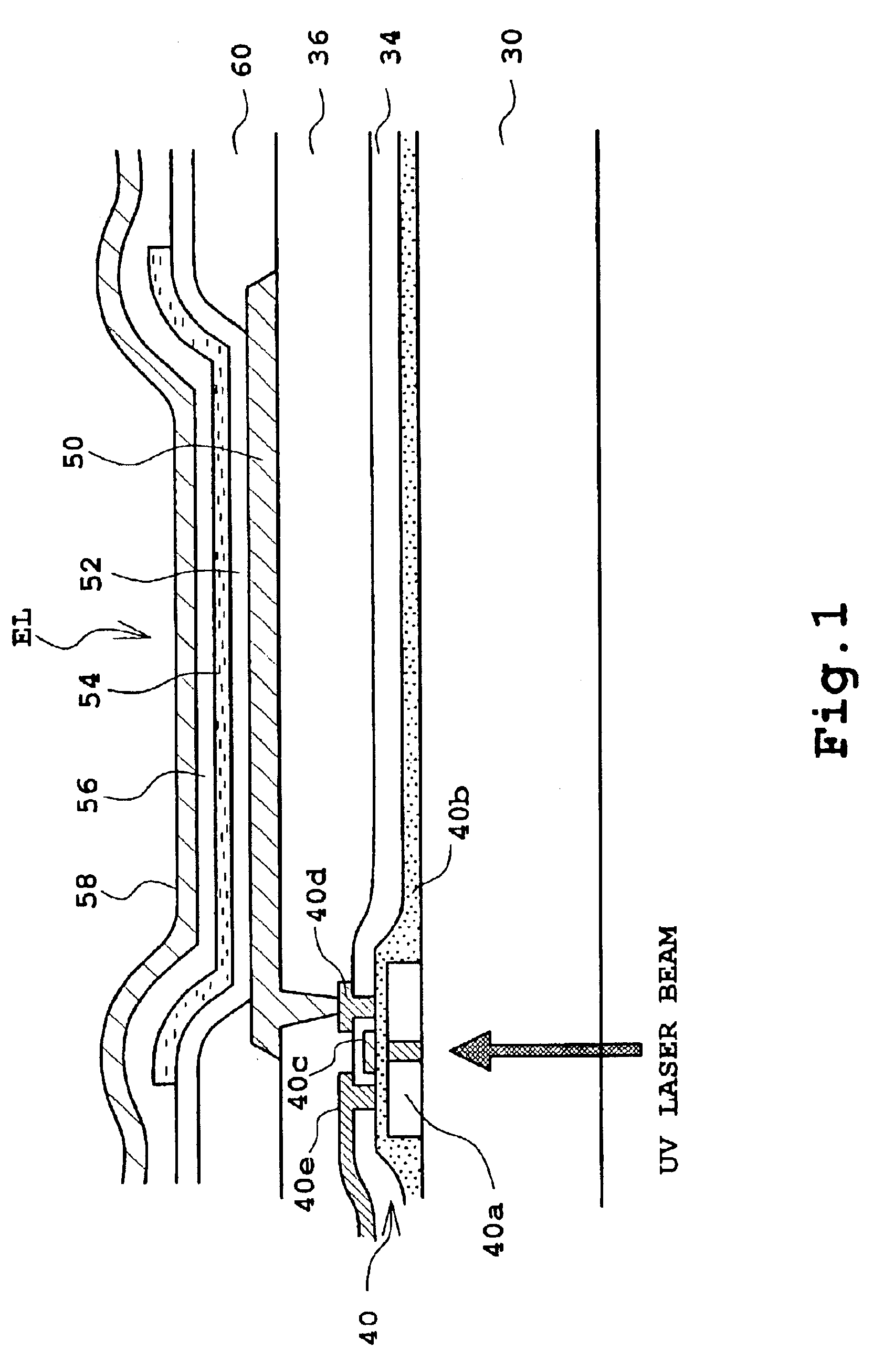
In this first example of the embodiment, a laser beam is irradiated from the underside of a gate electrode of a TFT, so as to allow the laser beam to cause micro-ablation in a semiconductor layer composed of polysilicon positioned beneath the gate electrode. Crystallinity of the semiconductor layer is thereby disintegrated to increase its resistance and lock the TFT in the OFF state. It should be noted that the laser beam is reflected by the gate electrode, such that the laser beam is effectively irradiated on the semiconductor layer without causing undesirable influences in layers located above the gate electrode.

Preferably, the laser employed is an ultraviolet (UV) laser such as a 355 nm YAG laser or a 308 nm excimer laser. If the laser has a longer wavelength, ablation may also be caused in the gate electrode during the process for disintegrating the semiconductor lay...


PUM


Abstract

A UV laser beam is selectively irradiated on an active layer (semiconductor layer) of a second TFT in a pixel, so as to degrade crystallinity of the active layer and thereby execute electrical disconnection. According to this method, dimming out of pixels can be performed without generating undesirable influences in other components. By directing the laser beam to a portion of the active layer located beneath the gate electrode, the laser beam can be reflected by the gate electrode, allowing execution of a more efficient laser irradiation.

Description

1. Field of the InventionThe present invention relates to the repairing of a defective pixel in an electroluminescence (EL) panel.2. Description of the Related ArtOne known type of flat display panel is an EL display panel. As opposed to a liquid crystal display (LCD) panel, an EL display panel is self-emissive. For that reason, and because EL display panels are flat and capable of bright, clear displays, their use is expected to spread widely. In particular, because organic EL elements can be driven at lower voltages compared to inorganic EL elements, widespread use of organic EL elements in various displays is anticipated.An organic EL display is configured by arranging, in a matrix, a large number of pixels each composed of an organic EL element. While either a passive or active method can be used to drive an organic EL element, use of an active matrix method is considered preferable, as is the case with LCDs. More specifically, in an active matrix method, a switching element is ...

Claims


Application Information

Patent Timeline
Patent Type & Authority Patents(United States)
IPC IPC(8): H01L27/32H01L27/28H01L51/56H01L51/50
CPCH01L51/56H01L27/3244G09G2330/10H01L2251/568H10K59/12H10K71/861H10K71/00H05B33/10
Inventor JINNO, YUSHI
Owner SANYO ELECTRIC CO LTD
Why Eureka
Try Eureka