Impedance trimming circuit

Inactive Publication Date: 2004-12-28
KK TOSHIBA
View PDF7 Cites 55 Cited by
  • Summary
  • Abstract
  • Description
  • Claims
  • Application Information

AI Technical Summary

Problems solved by technology

However, with this method, the circuit is affected by various variation factors such as a variation in reference voltage, an input offset voltage at the operational amplifier, a variation in the current ratio of a current source composed of the P channel MOS transistors, and a variation in MOS resistance.
Thus, actually, it is difficult to accurately adjust the output impedance.
For example, if the current ratio of the current sou

Method used


Image

  • Impedance trimming circuit
  • Impedance trimming circuit
  • Impedance trimming circuit

Examples


example 2

(3) Example 2 of the circuit

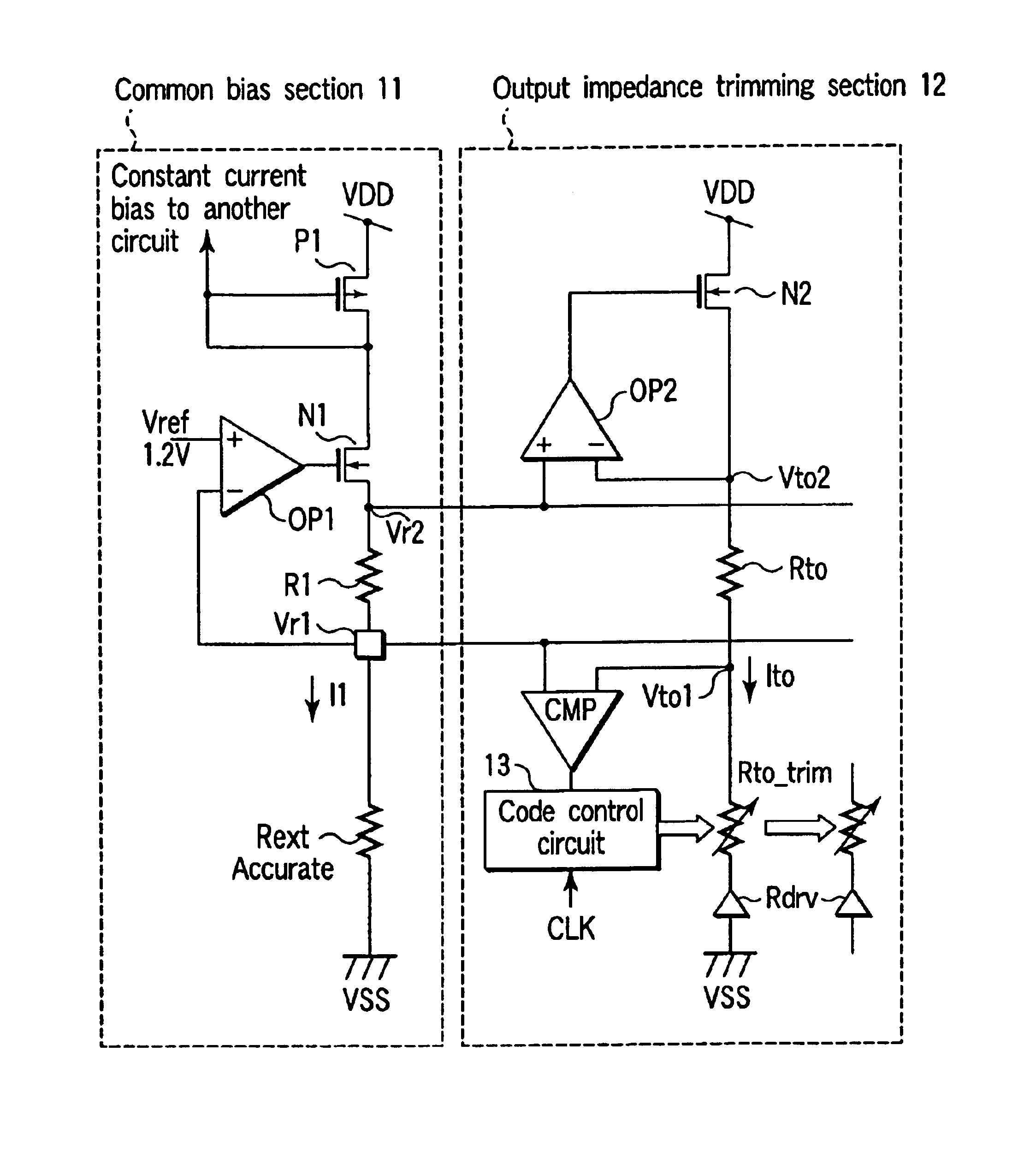
FIG. 28 shows example 2 of the impedance trimming circuit according to the ninth embodiment of the present invention.

The impedance trimming circuit provided as example 2 is an input impedance trimming circuit. This circuit does not need the driver dummy resistor or the driver, and merely performs trimming of the resistor, and adjusts the input impedance by using the obtained code, unlike the above output impedance trimming circuit.

Except the above points, an input impedance trimming circuit 14 does not greatly differ from the output impedance trimming section 12 shown in FIG. 22. Further, a code flattening circuit 16' of a code flattening section 15' is the same as the code flattening circuit 16 of the code flattening section 15 in FIG. 22.

first embodiment

The operation of the above input impedance trimming circuit is the same as that of the impedance trimming circuit and its explanation will be omitted.

example 3

(4) Example 3 of the circuit

FIG. 29 shows example 3 of the impedance trimming circuit according to the ninth embodiment of the present invention.

The impedance trimming circuit provided as example 3 is an input / output impedance trimming circuit. This circuit includes an output impedance trimming section 12 and an input impedance trimming section 14. In this case, a common bias section 11 is shared with the input impedance trimming section 12 and the output impedance trimming section 14.

The output impedance trimming section 12 and the code flattening section 15 are the same as the output impedance trimming section 12 and code flattering section 15 shown in FIG. 22. The input: impedance trimming section 14 and the code flattening section 15' are the same as the input impedance trimming section 14 and code flattening section 15' shown in FIG. 28.

The operation of the input / output impedance trimming circuit is the same as that of the impedance trimming circuit according to the first embod...


PUM


Abstract

A common bias section is composed of a first series circuit having an internal resistor and an external resistor connected in series and an operational amplifier having a first input terminal connected to a reference voltage, a second input terminal connected to a Vr1 node, and an output terminal connected to the series circuit. An impedance trimming section is composed of a series circuit having an internal resistor and an impedance dummy resistor connected in series, a comparator CMP having a first input terminal connected to the Vr1 node and a second input terminal connected to a Vto1 node, a code control circuit which uses a clock signal to latch an output signal from the comparator to generate a plurality of switching codes, and a switching circuit which switch a resistance value of the impedance dummy resistor.

Description

1. Field of the InventionThe present invention relates to an LSI containing an impedance trimming circuit to execute impedance matching on output impedance, input impedance, terminal resistance, or the like to suppress reflection of signals, thus allowing high-speed serial signals of high quality to be transferred, and in particular, to a trimming circuit for accurate and automatic adjustment.2. Description of the Related ArtFor a high-speed interface such as a USB2.0 (480 Mbps) or an LUDS (several Gbps), it has hitherto been essential to match input impedance, drive impedance, pull-up / pull-down resistance, or the like with a corresponding standard value (for example, .+-.10%) in order to suppress reflection of the waveform of a transferred signal, thus allowing a high-speed signal of high quality to be transmitted.However, resistance elements manufactured using an LSI manufacturing process vary markedly (for example, .+-.20%). Further, the on resistance of an output transistor depe...

Claims


Application Information

Patent Timeline
IPC IPC(8): H03H11/28H03H11/02
CPCH03H11/28
Inventor KITAGAWA, NOBUTAKATAKADA, SHUICHISASAKI, NOBUYUKIKAMINOTA, YASUHIKO
Owner KK TOSHIBA
Why Eureka
Try Eureka