Compositions for anti-reflective light absorbing layer and method for forming patterns in semiconductor device using the same

Inactive Publication Date: 2005-01-04
SAMSUNG ELECTRONICS CO LTD
View PDF8 Cites 16 Cited by
  • Summary
  • Abstract
  • Description
  • Claims
  • Application Information

AI Technical Summary

Benefits of technology

It is another feature of an embodiment of the present invention to provide a method for forming patterns in a semiconductor device using the anti-reflective light absorbing layer composition, in which a photoresist layer and the anti-reflective light absorbing layer are simultaneously developed after exposure of the photoresist layer, so that consumption of the photoresist layer during removal of the anti-reflective light absorbing layer is prevented.
The anti-reflective light absorbing layer composition according to the present invention is advantageous when used to form an anti-reflective layer that is required to form patterns in a semiconductor device by photolithography. The anti-reflective layer formed of the composition according to the present invention and a resist layer are simultaneously developed after exposure of the photoresist layer, so that a process of removing the anti-reflective layer by etching is unnecessary. As a result, consumption of the photoresist layer may be effectively prevented, and thus there is no need to increase the thickness of the photoresist layer.

Problems solved by technology

However, the organic reflective coating is similar to photoresist materials in its basic chemical structure and has a low etching selectivity with respect to a photoresist layer during dry etching.
As a result, during etching to remove the organic anti-reflective coating, consumption of the photoresist layer is increased.
In view of this, the thickness of the photoresist layer for photolithography is limited by the incorporation of the organic anti-reflective layer.

Method used


Image

  • Compositions for anti-reflective light absorbing layer and method for forming patterns in semiconductor device using the same
  • Compositions for anti-reflective light absorbing layer and method for forming patterns in semiconductor device using the same
  • Compositions for anti-reflective light absorbing layer and method for forming patterns in semiconductor device using the same

Examples


Embodiment Construction

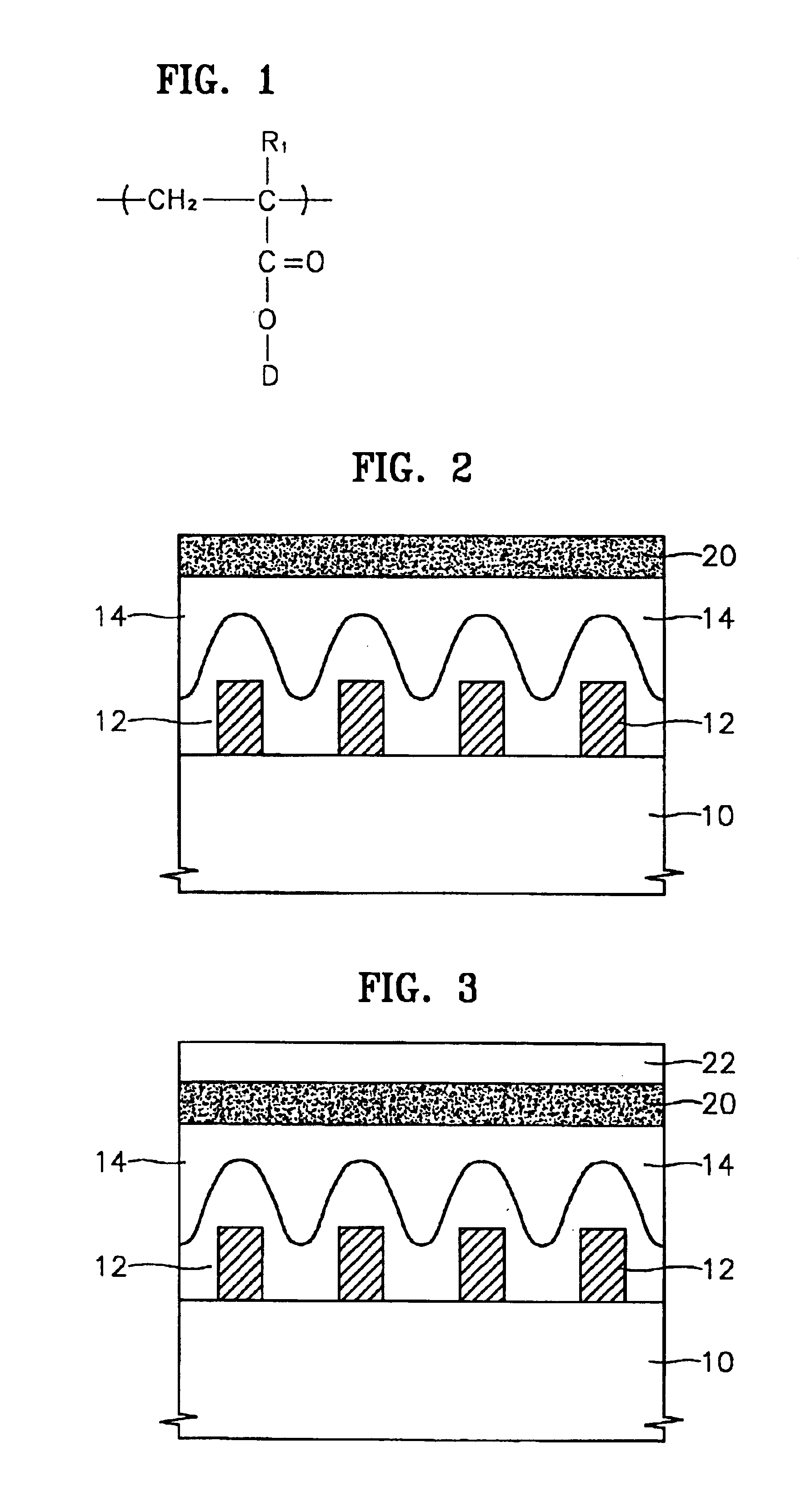
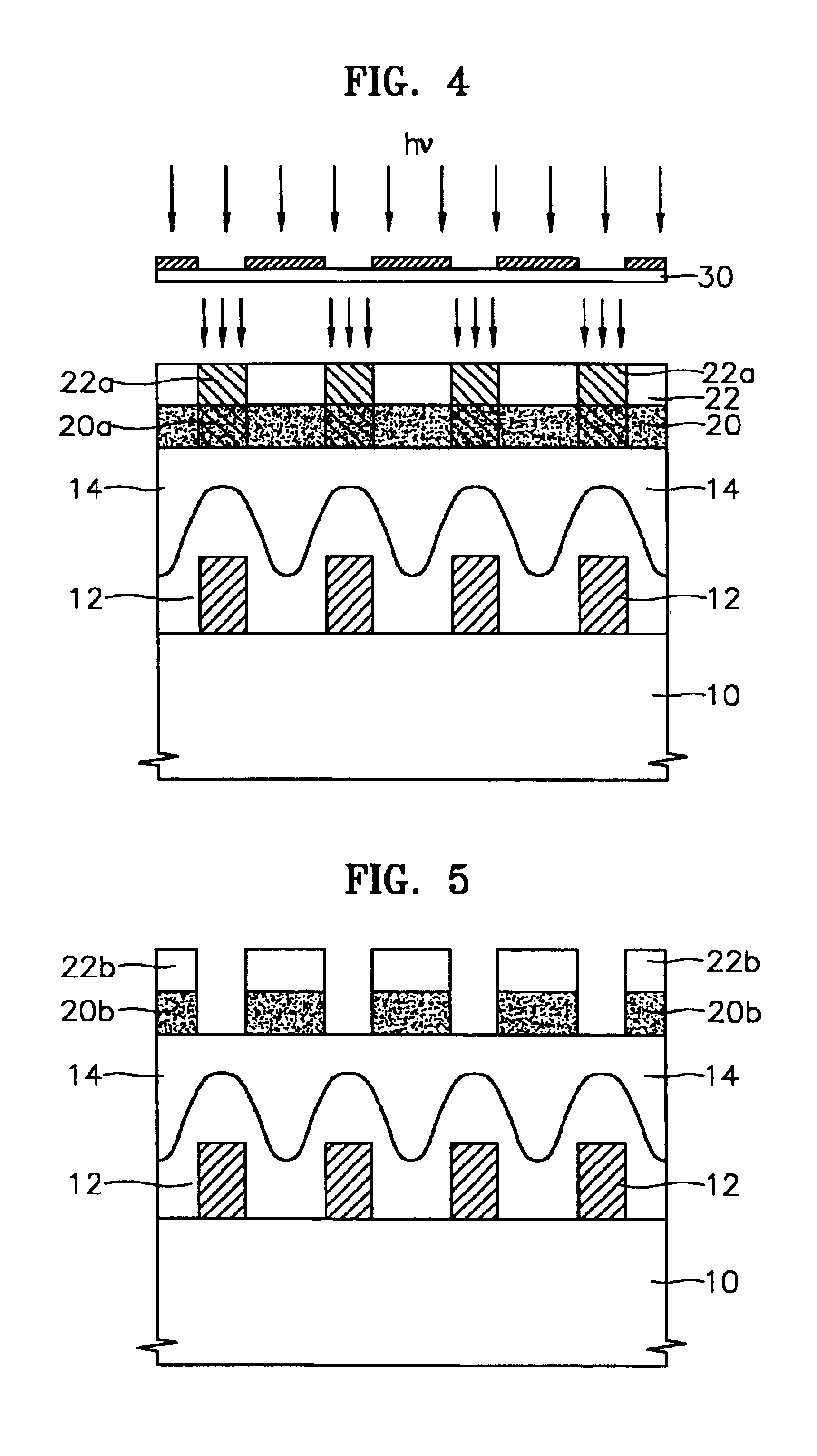
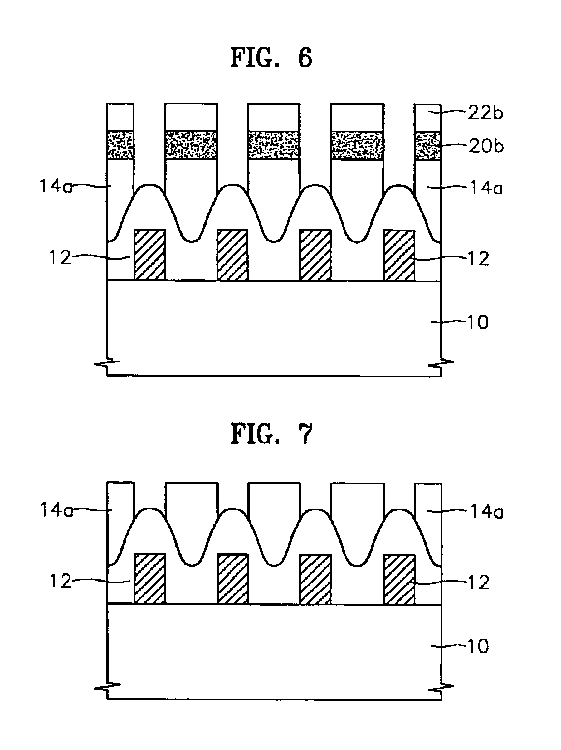
A composition for an anti-reflective light absorbing layer according to an embodiment of the present invention basically comprises in its structure a polymer having a predetermined light-absorptive repeating unit. A light-absorbing group is chemically bound to a side chain of the light-absorptive repeating unit of the polymer. The anti-reflective light absorbing layer composition according to the present invention comprises a photoacid generator and a cross-linker. The photoacid generator generates acid by using light during exposure to decompose the cross-linking of the polymer so that the polymer may be developed after the exposure. The cross-linker thermally cross-links the polymer and may be coupled to a side chain of the polymer to be decomposed from the cross-linked polymer by an acid. A catalyst is used to accelerate the cross-linking reaction of the polymer by the cross-linker.

FIG. 1 shows an example of a structure of a light-absorptive repeating unit of a polymer contained ...


PUM

PropertyMeasurementUnit
Temperatureaaaaaaaaaa
Percent by massaaaaaaaaaa

Abstract

A composition for an anti-reflective layer capable of simultaneously being developed together with a photoresist layer after exposure of the photoresist layer in a photolithography process and a method for forming patterns in a semiconductor device using the composition, wherein the anti-reflective light absorbing layer composition includes a polymer having a (meth)acrylate repeating unit, a light-absorbing group of diazoquinones chemically bound to the (meth)acrylate repeating unit, a photoacid generator, a cross-linker which thermally cross-links the polymer and is decomposed from the polymer by an acid, and a catalyst for the cross-linking reaction of the polymer. The method for forming patterns in a semiconductor device involves forming an anti-reflective layer on a semiconductor substrate using the composition and simultaneously exposing the anti-reflective layer and a photoresist layer, thereby chemically transforming the anti-reflective layer so it is able to be developed. The anti-reflective layer and the photoresist layer are simultaneously developed.

Description

BACKGROUND OF THE INVENTION1. Field of the InventionThe present invention relates to a light absorbing layer composition and a method for fabricating a semiconductor device using the composition. More particularly, the present invention relates to a composition for an anti-reflective light absorbing layer capable of preventing light reflection from a substrate during exposure in a photolithography process during the manufacture of an integrated circuit device and a method for forming patterns in a semiconductor device using the composition.2. Description of the Related ArtWith trends towards high-density semiconductor devices, a micro-process for forming ultrafine patterns, recently on submicron levels, in a photolithography process has been developed. In a lithography process, a photoresist layer is coated on a substrate and subjected to exposure and development processes to form a mask pattern. In general, the substrate has high-reflectivity material layers thereon. Accordingly, l...

Claims


Application Information

Patent Timeline
IPC IPC(8): G03F7/038G03F7/095G03F7/09G03F7/004G03F7/023G03F7/11H01L21/027
CPCG03F7/0382G03F7/095G03F7/091G03F7/405G03F7/0752G03F7/0757C09D183/04
Inventor YOON, SANG-WOONGCHUNG, HOE-SIKRYU, JIN-AKIM, YOUNG-HO
Owner SAMSUNG ELECTRONICS CO LTD
Why Eureka
Try Eureka