Method of patterning a substrate

a substrate and patterning technology, applied in non-linear optics, instruments, optics, etc., can solve the problems of reducing the accuracy of registration, and increasing the process cost of lithography, so as to achieve the effect of reducing the number of steps, increasing the process cost, and reducing the sensitivity of the method

Inactive Publication Date: 2005-01-04
SEIKO EPSON CORP
View PDF3 Cites 75 Cited by
  • Summary
  • Abstract
  • Description
  • Claims
  • Application Information

AI Technical Summary

Benefits of technology

[0012]In practice, photolithography has previously been used to form the PI strip. However, the use of lithography entails many steps including the application of a primer, coating of a photoresist, mask-alignment, exposure, baking, development, etching and stripping. The use of lithography therefore significantly increases process costs and outweighs the benefits of inkjet printing. Micro-contact printing and micro-moulding printing with an elastic stamp (mould), for example made of PDMS (polydimethylsiloxane) could also be used for pre-patterning, but the distortion and deformation of the elastic stamp discussed above deteriorates accuracy in registration. As an alternative, the recently developed method of photo-induced wettability patterning appears promising since it can be expected to involve a smaller number of steps than lithography. However, this method has not yet been properly established. In particular, in the current state of the art of this method, the wavelength of the light is too short and the sensitivity of the method is too low for realistic application.

Problems solved by technology

The use of lithography therefore significantly increases process costs and outweighs the benefits of inkjet printing.
Micro-contact printing and micro-moulding printing with an elastic stamp (mould), for example made of PDMS (polydimethylsiloxane) could also be used for pre-patterning, but the distortion and deformation of the elastic stamp discussed above deteriorates accuracy in registration.
However, this method has not yet been properly established.
In particular, in the current state of the art of this method, the wavelength of the light is too short and the sensitivity of the method is too low for realistic application.
Thus, there is no suitable technique for consistently providing sufficiently small channel lengths in a cost effective manner.

Method used


Image

  • Method of patterning a substrate
  • Method of patterning a substrate
  • Method of patterning a substrate

Examples


Embodiment Construction

IG. 10 shows a method of fabricating a plurality of thin film transistors in accordance with the present invention;

[0029]FIG. 11 shows a block diagram of an electro-optical device;

[0030]FIG. 12 shows a schematic view of a mobile personal computer incorporating a display and other devices fabricated in accordance with the present invention;

[0031]FIG. 13 shows a schematic view of a mobile telephone incorporating a display and other devices fabricated in accordance with the present invention; and

[0032]FIG. 14 shows a schematic view of a digital camera incorporating a display and other devices fabricated in accordance with the present invention.

DETAILED DESCRIPTION OF EXEMPLARY EMBODIMENTS

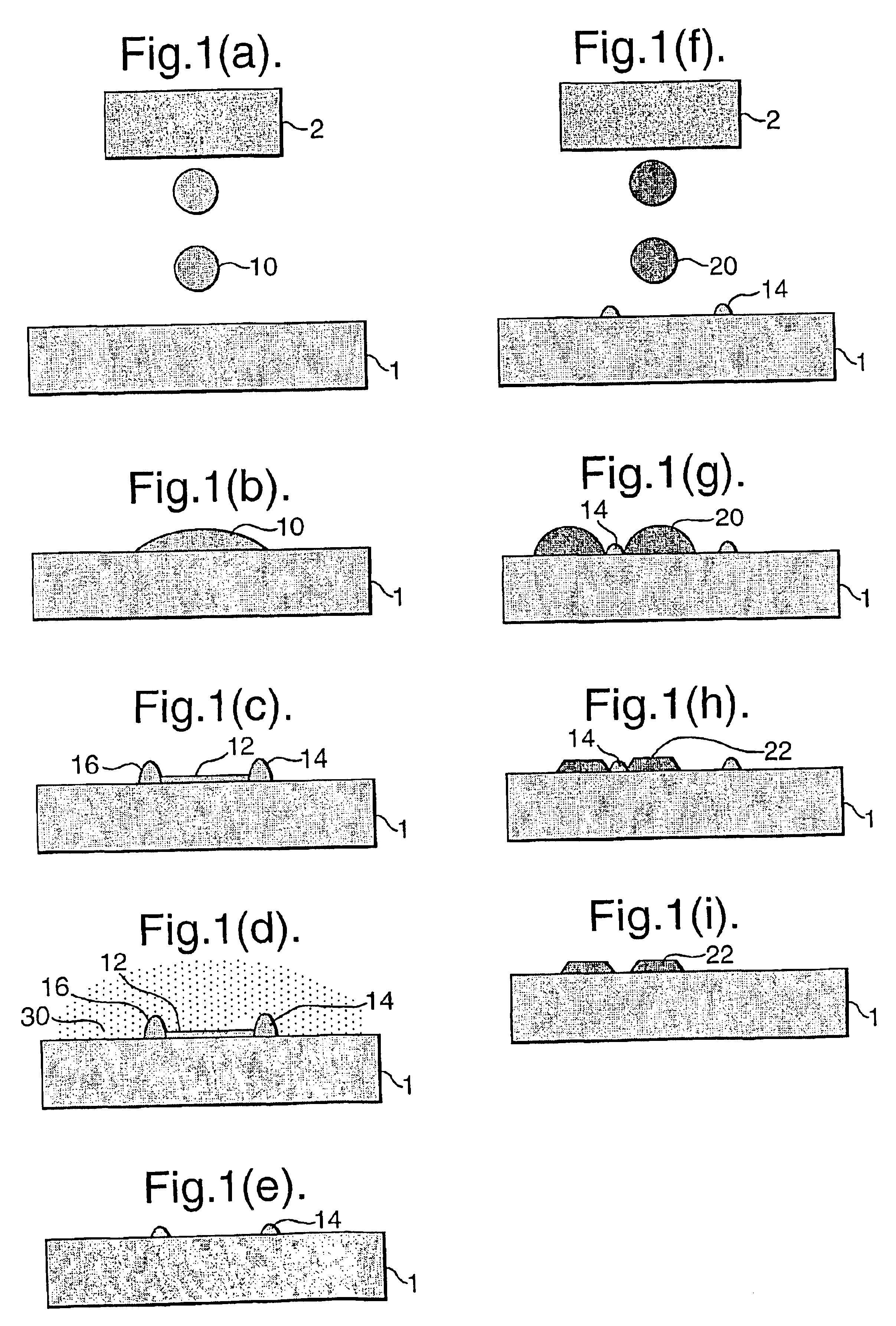
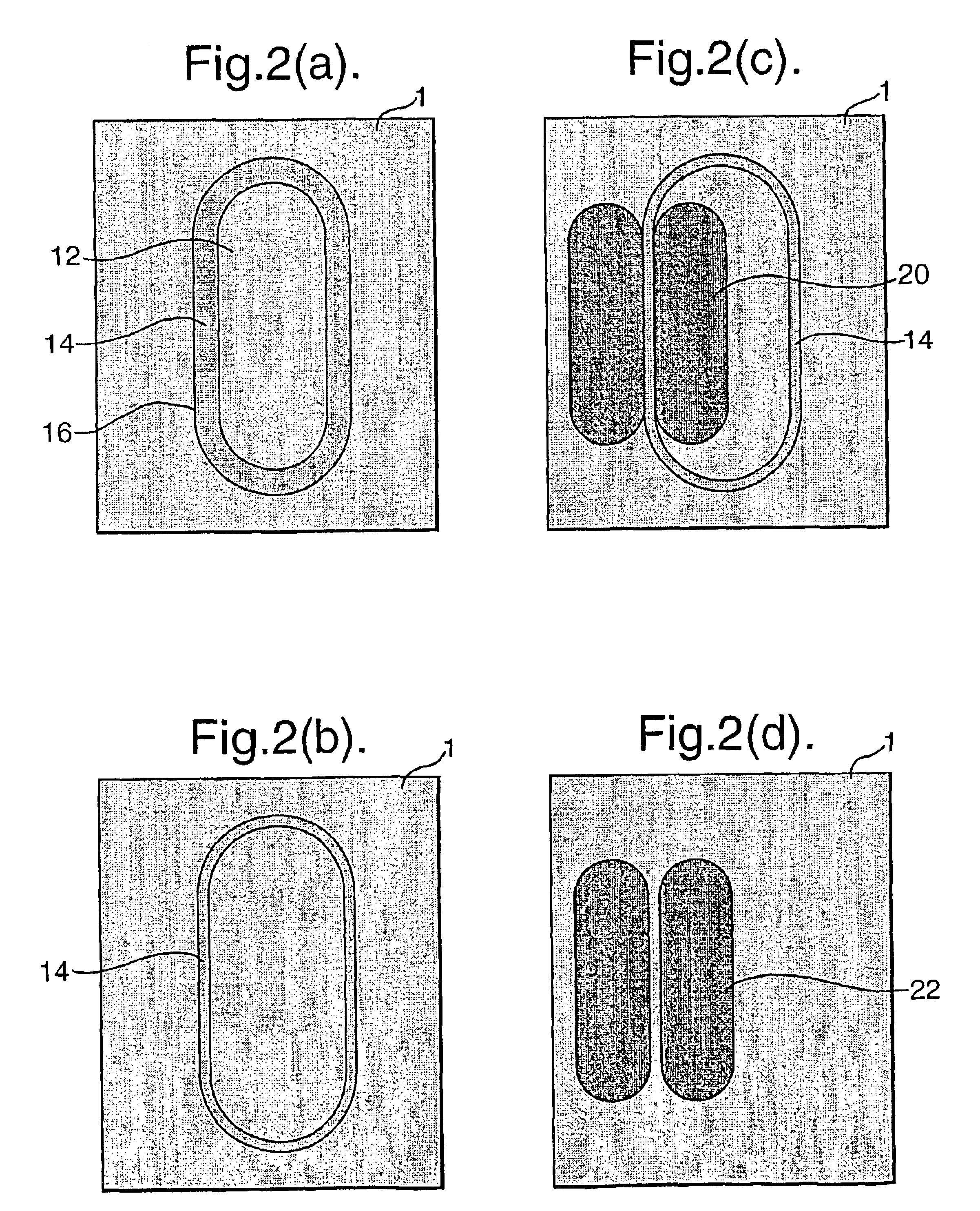
[0033]The present invention provides a high-resolution patterning technique that does not require photolithography or similar processes. Briefly, in one aspect of the present invention pre-patterning is formed with a first material, which is deposited on a substrate in the form of droplets of a solutio...


PUM


Abstract

The invention provides a method of pattering a substrate, in which a first material in solution is deposited on the substrate. The composition of the solution of the first material is selected so it dries to leave a residue of the first material on the substrate, the residue comprising a thin film in the centre and a ridge around the perimeter. The residue is etched to remove the thin film, leaving the ridge on the substrate. After etching the ridge is hydrophobic and the substrate is hydrophilic. An aqueous solution of a second material is then deposited on both sides of the ridge. After the aqueous solution has dried, the ridge is removed, leaving a layer of the second material on the substrate, the layer having a narrow gap therethrough. The layer may be used for the source and drain electrodes of an organic thin film transistor.

Description

BACKGROUND OF THE INVENTION[0002]1. Field of Invention[0003]The present invention relates to a method of patterning a substrate. In particular, the method of the present invention relates to patterning substrates to provide electronic devices such as thin film transistors (TFTs) and / or electro-optic devices thereon.[0004]2. Description of Related Art[0005]Photolithography is presently widely used for the mass production of electronic devices and achieves very high resolution and registration. In photolithography, a spin-coated photoresist layer is provided on a substrate and is exposed by blue or ultraviolet light with an aligner or stepper, which aligns patterns on a master, comprising a mask or reticule, with the substrate. The exposed photoresist is then developed to provide patterns of the photoresist on the substrate. This is generally followed by an etching or deposition process to pattern an objective material. The resolution achieved by photolithography is determined by the ...

Claims


Application Information

Patent Timeline
Patent Type & Authority Patents(United States)
IPC IPC(8): H01L51/40H01L51/05H01L51/50H01L21/288H01L21/336H01L29/786H01L51/00H05B33/14
CPCH01L51/0005H01L51/0022H01L51/0541H01L51/0516H10K71/135H10K71/611H10K10/468H10K10/464G02F1/13
Inventor TAKEO, KAWASE
Owner SEIKO EPSON CORP
Why Eureka
Try Eureka