I/O buffer with variable conductivity

a buffer circuit and variable conductivity technology, applied in the direction of voltage/current interference elimination, pulse technique, reliability increasing modifications, etc., can solve the problems of incorrect determination and action, affecting the normal operation of the circuit, and incorrect judgment of data levels by the receiver, so as to improve the i/o buffer driver circuit, the conductivity of the cmos transistor is first increased, and the conductivity is gradually reduced.

Inactive Publication Date: 2005-01-04
VIA TECH INC
View PDF7 Cites 13 Cited by
  • Summary
  • Abstract
  • Description
  • Claims
  • Application Information

AI Technical Summary

Benefits of technology

In observation of the unstable phenomena occurred to the receive end during the SSO transitions that may result in incorrect actions of circuit operations, the invention thus improves the I/O buffer driver circuit. The invention uses a delay circuit in combination with a CMOS transistor driver to change the conductivity characteristic of the output signals. When the I/O output signals make transitio...

Problems solved by technology

Such noise signal produced by the SSO will cause incorrect judgment on data levels by the receiver.
Such incorrect determinations and acti...

Method used


Image

  • I/O buffer with variable conductivity
  • I/O buffer with variable conductivity
  • I/O buffer with variable conductivity

Examples


Embodiment Construction

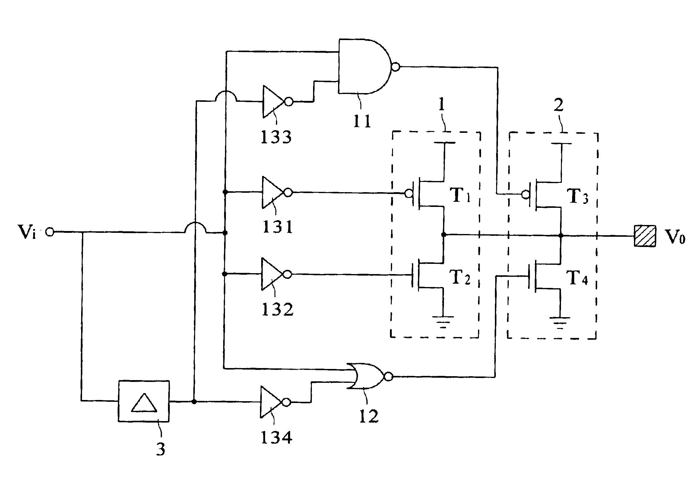
With reference to FIG. 4, the I / O buffer with variable conductivity of the present invention includes a pre-push-pull driver 1 and a post-push-pull driver 2. The input signals of pre-push-pull driver 1 and the post-push-pull driver 2 are connected with a delay circuit 3 in series, so that the two input signals have a delayed phase difference. The pre-push-pull driver 1 and post-push-pull driver 2 drive the output signal Vo in the delayed phase difference to provide the desired variable conductivity.

When the input signal Vi makes a transition, the pre-push-pull drive 1 and post-push-pull driver 2 simultaneously drive the output signal Vo to provide larger conductivity. Due to the effect of the delay circuit 3, the post-push-pull driver 2 stops driving after a delay time following the transition of the input signal Vi. The conductivity of the output signal Vo is thus changed to provide a smaller conductivity, inhibiting the increase of the load current i and preventing the overshootin...


PUM


Abstract

A driver structure for an I/O buffer circuit is disclosed. The driver structure includes a pre-push-pull driver and a post-push-pull driver. A delay circuit along is connected in series between the input signals of the pre-push-pull driver and the post-push-pull driver. After a delay time following a transition of the input signal, the circuit operation of the post-push-pull driver is turned off before the amplitude of the output signal reaches its maximum overshooting. This changes the output conductivity to inhibit the overshooting in the output signal, preventing power bounce and ground bounce at the receiving end.

Description

BACKGROUND OF THE INVENTION1. Field of InventionThe invention relates to an I / O (Input / Output) buffer circuit. More particular, the invention pertains to an I / O buffer circuit with variable conductivity, which can improve the data integrity and decrease signal wave deformation during SSO (Simultaneous Switching Output).2. Related ArtWith reference to FIG. 1, the conventional I / O buffer circuit is a push-pull driver comprised of a PMOS (P-type Metal Oxide Semiconductor) transistor T1 and an NMOS (N-type Metal Oxide Semiconductor) transistor T2. The transistors T1 and T2 are connected between a work voltage Vdd and the ground Gnd in series. The input signal Vi passes through two NOT gates 13 to reach the gates of the transistors T1 and T2. The drains of the transistors T1 and T2 are both connected to the output terminal pad, output signal Vo. When the input signal Vi has a Hi voltage, it is inverted by the NOT gate 13 into a Lo voltage. The transistor T1 called a pull-up transistor be...

Claims


Application Information

Patent Timeline
IPC IPC(8): H03K17/16H03K19/003
CPCH03K19/00361H03K17/164
Inventor YEN, ANDREW
Owner VIA TECH INC
Why Eureka
Try Eureka