Bulk input differential logic circuit

Inactive Publication Date: 2005-01-04
IND TECH RES INST
View PDF3 Cites 16 Cited by
  • Summary
  • Abstract
  • Description
  • Claims
  • Application Information

AI Technical Summary

Benefits of technology

The object of the present invention is to provide a new bulk input differential logic circuit composed of a current latch sense amplifier and a MOS logic circuit in which bulk transistors are used as terminals for input

Problems solved by technology

However, it has a disadvantage in that 2n transistors are needed to implement a n-input NOR gate.
The most serious problem with this circuit is that the terminal Vo is not biased by a DC voltage, which may result in wrong output due t

Method used


Image

  • Bulk input differential logic circuit
  • Bulk input differential logic circuit
  • Bulk input differential logic circuit

Examples


first embodiment

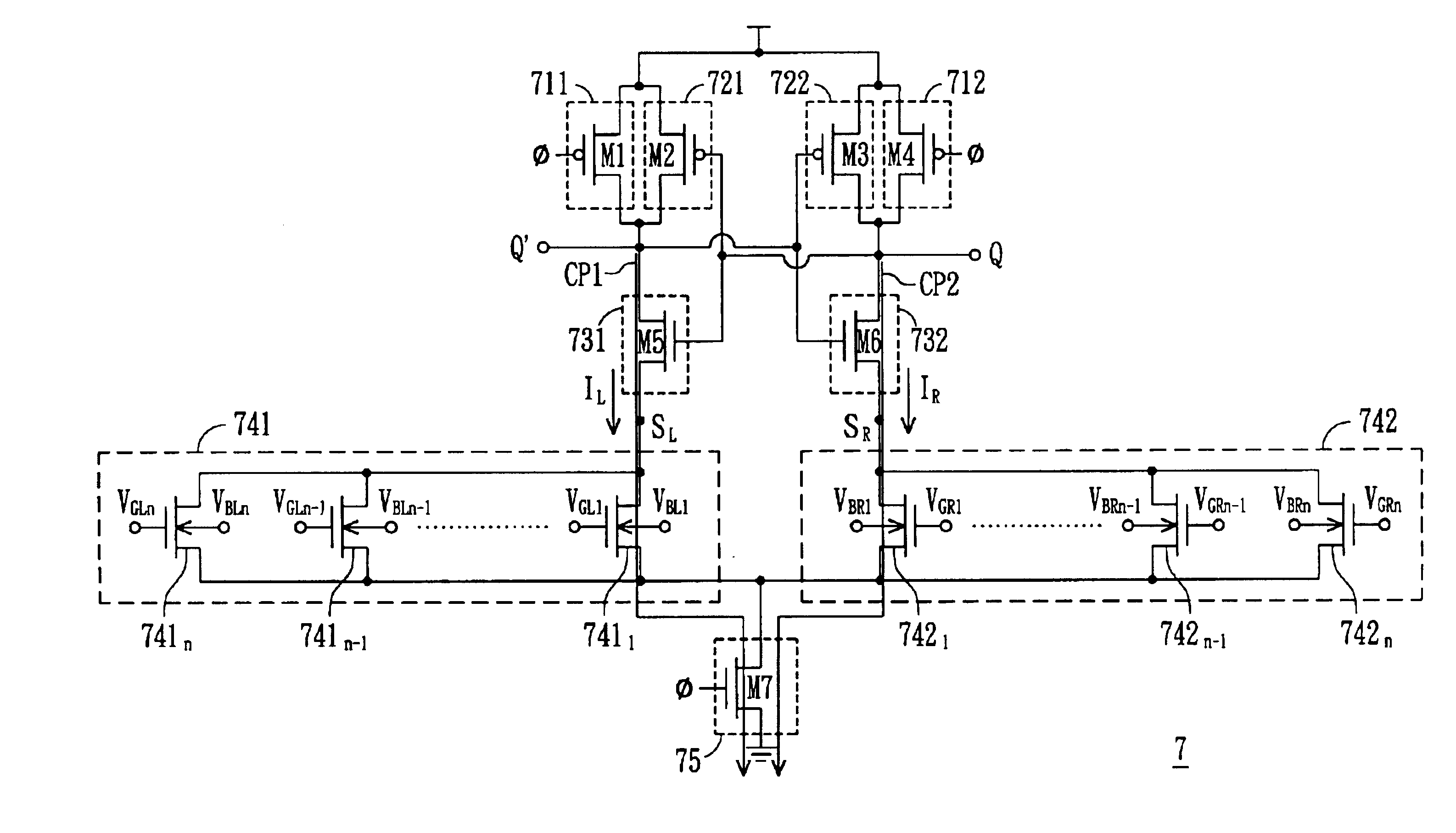
FIG. 7 is a diagram showing a bulk input differential logic circuit according to the invention. Two current paths CP1 and CP2 are formed in the bulk input differential logic circuit 7. The current paths CP1 and CP2 are respectively connected between terminals Q and Q′, and the ground. The bulk input differential logic circuit 7 includes seven switches 711, 712, 721, 722, 731, 732 and 75, and two NMOS logic circuit 741 and 742. The switch 731, NMOS logic circuit 741 and switch 75 form the current path CP1 while the switch 732, NMOS logic circuit 742 and switch 75 form the current path CP2. The terminals Q and Q′ are respectively between the switches 721 and 731, and the switches 722 and 732.

Both of the switches 711 and 712 are controlled by a clock signal φ. They are opened when the clock signal φ is at a logic High and are closed when the clock signal φ is at a logic Low. The switches 711 and 712 are composed of P-type transistors M1 and M4 having gates coupled to receive the clock ...

second embodiment

FIG. 14A is a diagram showing a bulk input differential logic circuit according to the invention. The bulk input differential logic circuit includes four P-type transistors 151, 152, 155 and 156, five N-type transistors 153, 157, 159, 1581 and 1541, and a boost circuit composed of transistors 91 and 101. The P-type transistors 151, 152 have drains commonly coupled to receive the logic High voltage, sources commonly coupled to the terminal Q′, and gates respectively coupled to receive a clock signal φ and the terminal Q. The P-type transistors 155 and 156 have drains commonly coupled to receive the logic High voltage, sources commonly coupled to the terminal Q, and gates respectively coupled to the terminal Q and to receive the clock signal φ. The N-type transistors 153 and 157 have drains respectively coupled to the terminal Q′ and Q, and gates respectively coupled to the terminals Q and Q′. The N-type transistor 1541 has a drain coupled to the source of the N-type transistor 153, a...

third embodiment

FIG. 15A is a diagram showing a bulk input differential logic circuit according to the invention. The bulk input differential logic circuit includes four P-type transistors 161, 162, 165 and 166, six N-type transistors 163, 167, 169, 1681, 1641 and 1642, and a boost circuit composed of transistors 91 and 101. It is noted that the circuit shown in FIG. 15A is similar to that in FIG. 14A except that the circuit in FIG. 15A has the transistors 1641 and 1642 receiving the input signals A, A′, B and B′.

FIG. 15B shows a truth table of the bulk input logic circuit in FIG. 15A. Therefrom, the bulk input logic circuit in FIG. 15A implements XOR operation of the signals A and B.


PUM


Abstract

A bulk input differential logic circuit. The circuit outputs a large signal high enough to assert a logic High and Low by variations of the threshold voltage controlled by the bulk input signal and amplification of the sense amplifier. A boost circuit is disposed on the bulk input terminal, which may receive multiple bulk input signals. This makes it possible to use fewer circuit elements and smaller circuit area for a complicated logic operation.

Description

BACKGROUND OF THE INVENTION1. Field of the InventionThe present invention relates to a logic circuit and particularly to a bulk input differential logic circuit with fewer circuit elements for a complicated logic and high speed operation.2. Description of the Prior ArtFIG. 1 is a diagram showing a static CMOS circuit of a 3-input NOR gate. It includes three P-type transistors 111, 112 and 113 having gates receiving signals A, B and C respectively, and three N-type transistors 121, 122 and 123 connected in parallel having gates receiving the signals A, B and C respectively. One of the N-type transistors 121, 122 and 123 is turned on and a logic Low is output on the terminal Vo if one of the signals A, B, and C carries a logic High. All of the P-type transistors 111, 112 and 113 are turned on and a logic High is output on the terminal Vo if all of the signals A, B, and C carry a logic Low. This circuit has an advantage in that there is no DC power consumption. However, it has a disadv...

Claims


Application Information

Patent Timeline
IPC IPC(8): H03K19/21H03K19/096H03K19/017H03K19/01H03K19/20
CPCH03K19/01707H03K19/215H03K19/0963
Inventor HUANG, HONG-YILIN, JING-FU
Owner IND TECH RES INST
Why Eureka
Try Eureka