Low power consumption MIS semiconductor device

a technology of semiconductor devices and low power consumption, applied in the direction of power consumption reduction, pulse technique, instruments, etc., can solve the problems of disadvantageous standby current increase, off-leak current increase, and the threshold voltage cannot be reduced in absolute value, so as to reduce the current dissipation and simple circuit configuration

Inactive Publication Date: 2008-04-08
RENESAS ELECTRONICS CORP
View PDF39 Cites 81 Cited by
  • Summary
  • Abstract
  • Description
  • Claims
  • Application Information

AI Technical Summary

Benefits of technology

[0035]It is an object of the present invention to provide a semiconductor device capable of reducing a current dissipation in a standby state with a simple circuit configuration.
[0036]It is another object of the present invention to provide a semiconductor device capable of more reliably reducing a current consumed in a standby state and of achieving a high speed operation in transition to an active cycle.
[0040]According to the arrangements as described above, a power source line can be reinforced in an active cycle and a logic circuit can quickly be operated and the power supply switching transistor can be reliably kept in an off state to reduce a leak current during a standby state.

Problems solved by technology

However, a threshold voltage cannot be reduced in absolute value in accordance with the scaling rule.
Accordingly, in a standby cycle in which MIS transistor is kept off, the off-leak current increases and a standby current increases disadvantageously.
In particular, for portable equipment or other battery-driven equipment employing such a semiconductor device, reducing the off-leak current is a significant issue to increase the lifetime of a battery.
If a gate insulation film is reduced in thickness as an operating power supply voltage is reduced, e.g., the gate insulation film is reduced to substantially 3 nm under the condition of a power supply voltage of no more than 1.5V, a tunneling current flows through the gate insulation film of the MIS transistor in the on state (conductive state) and a power source current through the transistor in the on state increases disadvantageously.
Holes are moved away from the interface with the insulation film, to cause the poor state of majority carriers (holes).
This issue of disadvantageous gate tunnel current similarly applied to an n type substrate region, with the modification that the gate receives a voltage opposite in polarity and the energy band bends in the opposite directions.
Thus, if an operating power supply voltage is decreased and a gate insulation film is reduced in thickness in accordance with a scaling rule, this gate tunnel current attains an insignificant, significant value and accordingly, a current consumed in the standby cycle increases.
Thus, it is necessary to determine a circuit operation timing with a worst case considered, and high speed and stable operation cannot be achieved.
This results in a disadvantageously increased layout area in the case of an increased number of stages of inverters IVa and IVb.
In particular, if power supply noise is generated, the noise cannot be absorbed rapidly, a circuit cannot be operated stably, and the noise reduces a circuit operating margin.
Furthermore, if driving ability of the power supply switching transistor cannot be increased sufficiently, the sub power supply and ground lines cannot be driven rapidly to prescribed voltage levels in transition from the off state to an on state.
Consequently, a certain period of time is required before an operation starts, which is an obstacle against high speed operation.

Method used


Image

  • Low power consumption MIS semiconductor device
  • Low power consumption MIS semiconductor device
  • Low power consumption MIS semiconductor device

Examples


first embodiment

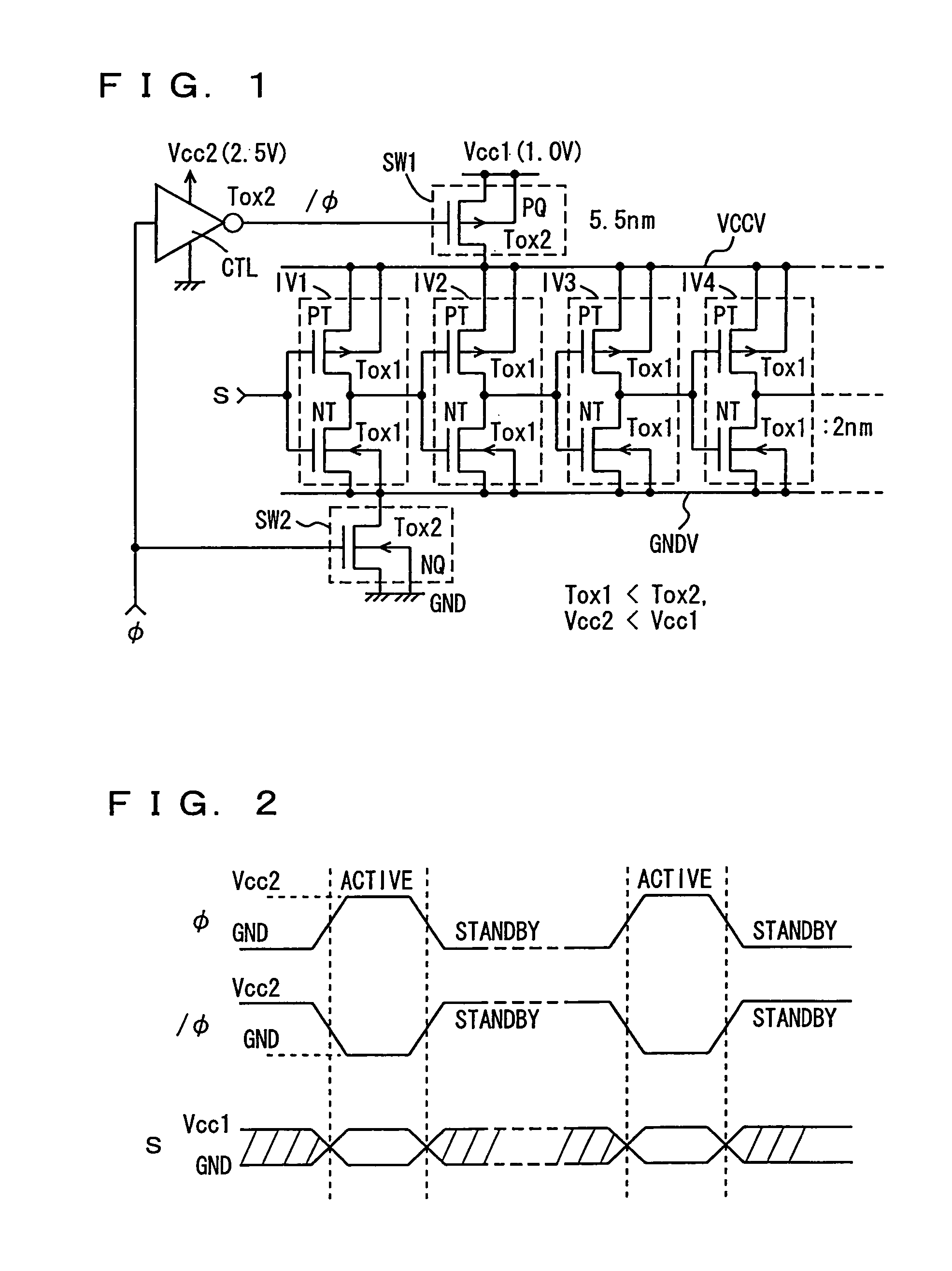
[0073]FIG. 1 shows a configuration of a semiconductor device according to the present invention in a first embodiment. In FIG. 1, the semiconductor device includes, as an internal function circuit, CMOS inverters IV1 to IV4 cascaded in four stages by way of example. CMOS inverters IV1 to IV4 each include a p channel MIS transistor PT and an n channel MIS transistor NT. MIS transistors PT and NT each have a gate insulation film having a thickness Tox1, for example, of 2 nm.

[0074]The p channel MIS transistors of CMOS inverters IV1 to IV4 have their respective sources and substrate regions (or backgates) connected commonly to a high-side virtual power source line (hereinafter simply referred to as a virtual power supply line) VCCV. The n channel MIS transistors of CMOS inverters IV1 to IV4 have their respective sources and substrate regions connected commonly to a low-side virtual power source line (hereinafter simply referred to as a virtual ground line) GNDV.

[0075]Virtual power suppl...

second embodiment

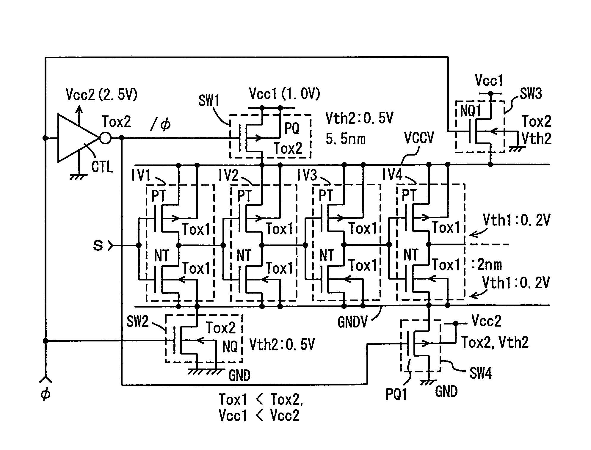
[0112]FIG. 8 shows a configuration of the semiconductor device according to a second embodiment of the present invention. The semiconductor device shown in FIG. 8 includes, in addition to the configuration of the semiconductor device shown in FIG. 1, a power supply switch circuit SW3 provided between a virtual power supply line VCCV and a power supply node receiving power supply voltage Vcc1 and a power supply switch circuit SW4 provided between virtual ground line GNDV and a ground node.

[0113]Power supply switch circuit SW3 is constructed of an n-channel MIS transistor NQ1 connected between a power supply node receiving power supply voltage Vcc1 and virtual power supply line VCCV, and having its gate receiving switch control signal φ and its backgate connected to a ground node. N channel MIS transistor NQ1 has a gate insulation film of thickness Tox2.

[0114]Power supply switch circuit SW4 is constructed of a p channel MIS transistor PQ1 connected between virtual ground line GNDV and...

third embodiment

[0132]FIG. 10 shows a configuration of the semiconductor device according to the present invention in a third embodiment. The semiconductor device shown in FIG. 10 differs in configuration from the semiconductor device shown in FIG. 1 in the following points. The amount of dopant doped into the channel of a p channel MIS transistor PQ31 constructing power supply switch circuit SW1 is made equal to that of dopant into the channel of a p channel MIS transistor PT of CMOS inverters IV1 to IV4. MIS transistors PQ31 and PT have their respective gate insulation films of the thickness the same as described in the first embodiment, i.e., Tox2 and Tox1, respectively.

[0133]In addition, the amount of dopant doped into the channel of an n channel MIS transistor NQ31 constructing power supply switch circuit SW2 is equal to the amount of dopant doped into the channel of an n channel MIS transistor NT of CMOS inverters IV1 to IV4. MIS transistors NT and NQ31 have their respective gate insulation f...


PUM


Abstract

A logic gate is constructed of an insulated gate field effect transistor (MIS transistor) having a thin gate insulation film. An operation power supply line to the logic gate is provided with an MIS transistor having a thick gate insulation film for switching the supply and stop of an operation power source voltage. A voltage of the gate of the power source switching transistor is made changing in an amplitude greater than an amplitude of an input and an output signal to the logic gate. Current consumption in a semiconductor device configured of MIS transistor of a thin gate insulation film can be reduced and an power source voltage thereof can be stabilized.

Description

CROSS REFERENCES AND RELATED APPLICATIONS[0001]This application is a Divisional of U.S. patent application Ser. No. 10 / 409,585 filed on Apr. 9, 2003 now U.S. Pat. No. 7,042,245.BACKGROUND OF THE INVENTION[0002]1. Field of the Invention[0003]The present invention relates generally to semiconductor devices including an insulated gate field effect transistor (hereinafter referred to as an MIS transistor) and particularly to configurations for reducing power consumption in semiconductor devices having microfabricated CMOS transistors (p and n channel MIS transistors). More specifically, the present invention relates to configurations for reducing gate tunneling current of microfabricated MIS transistors.[0004]2. Description of the Background Art[0005]In CMOS semiconductor devices including CMOS transistors as a component, if an MIS transistor is significantly scaled down in size, an operating power supply voltage is reduced in order to ensure the reliability of the transistors and to ac...

Claims


Application Information

Patent Timeline
Patent Type & Authority Patents(United States)
IPC IPC(8): H03K19/20G05F1/10H01L21/822H01L21/8238H01L27/04H01L27/092H03K17/16H03K19/00H03K19/0948
CPCG11C5/147H03K19/0016H01L27/0922
Inventor HIDAKA, HIDETO
Owner RENESAS ELECTRONICS CORP
Why Eureka
Try Eureka