Three level inverter

a three-level inverter and pulse width technology, applied in pulse technique, process and machine control, instruments, etc., can solve the problems of low frequency, low cost, and significant switching loss of inverter transistors

Active Publication Date: 2005-01-04
AMERICA POWER CONVERSION CORP
View PDF10 Cites 146 Cited by
  • Summary
  • Abstract
  • Description
  • Claims
  • Application Information

AI Technical Summary

Benefits of technology

[0013]Another embodiment of the present invention is directed to a method of providing alternating current from an inverter. The method includes providing: a first voltage node coupled to a neutral DC voltage source via a first diode oriented to prevent under-voltage of the first voltage node; a second voltage node coupled to the neutral DC voltage source via a second diode oriented to prevent over-voltage of the second voltage node; an AC output node; a first bipolar transistor, having a first collector coupled to the first voltage node and a first emitter coupled to the AC output node, such that the first emitter and the first collector is bridged by a third diode in a direction that allows the third diode to conduct reverse currents; a second bipolar transistor, having a second collector coupled to the AC output node and a second emitter coupled to the second voltage node, wherein the second emitter and the second collector is bridged by a fourth diode in a direction that allows the fourth diode to conduct reverse currents; a first field effect transistor, having a first drain coupled to a positive DC voltage source and a first source coupled to the first voltage node; a second field effect transistor, having a second drain coupled to the second voltage node and a first source coupled to a negative DC voltage source; and a control system for turning on and off the field effect transistors and the bipolar transistors; and supplying control signals to the transistors that differ for each of four output phase quadrants. Additionally embodiments of this method are considered such that the control system includes methods for: modulating the first field effect transistor while the first bipolar transistor is in an on state and while the second field effect transistor is in an off state when the inverter is operated in a first output phase quadrant characterized by both output voltage and current being positive; modulating the first and second bipolar transistors while the first field effect transistor is in an off state and while the second field effect transistor is in an on state when the inverter is operated in a second output phase quadrant characterized by negative output voltage and positive output current; modulating the second field effect transistor while the second bipolar transistor is in an on state and while the first bipolar transistor and the first FET are in an off state when the inverter is operated in a third output phase quadrant characterized by both output voltage and current being negative; and modulating the first and second bipolar transistors while the first field effect transistor is in an on state and while the second field effect transistor is in an off state when the inverter is operated in a fourth output phase quadrant characterized by negative output voltage and positive output current. In at least one embodiment of the method described above, the second bipolar transistor is modulated during operation in the first phase quadrant and the first bipolar transistor is modulated during operation in the third phase quadrant. It is further considered that the bipolar transistors may be modulated such that both bipolar transistors are not closed simultaneously. It is also considered that the determination of the phase quadrant may be delayed until the output current polarity remains constant for more than one modulation cycle.

Problems solved by technology

While potentially low cost, there are some drawbacks associated with using two-level inverters.
This voltage swing can cause significant switching loss in the inverter transistors.
However, this frequency may be so low that it creates audible noise (<20 kHz) or excessive output ripple current.
A further drawback of two-level inverters is that the voltage output is typically derived directly from the switching bridge and may have a very high content of high frequency harmonics.
This may cause additional losses in the output filter when used in typical applications.
However, three-level inverters are typically more complex and expensive than two-level inverters.
MOSFETs are generally known to have very good switching performance, but the internal (anti-parallel) body-diode exhibits poor recovery behavior.
Poor recovery behavior of freewheeling diodes will produce undesirable effects such as high peak currents and / or oscillations when rapidly commutated (turned off).
The addition of these diodes significantly increases the cost of the inverter design and adds conduction losses.
IGBTs typically have poorer switching performance than MOSFETS, but require the addition of fewer diodes to provide rapid recovery behavior, since the internal series diode present in IGBTs allows the designer to add a single diode to the freewheeling path.
The use of an inductive or a capacitive load with an inverter can result in phase shifts between the output voltage and the output current.

Method used


Image

  • Three level inverter
  • Three level inverter
  • Three level inverter

Examples


Embodiment Construction

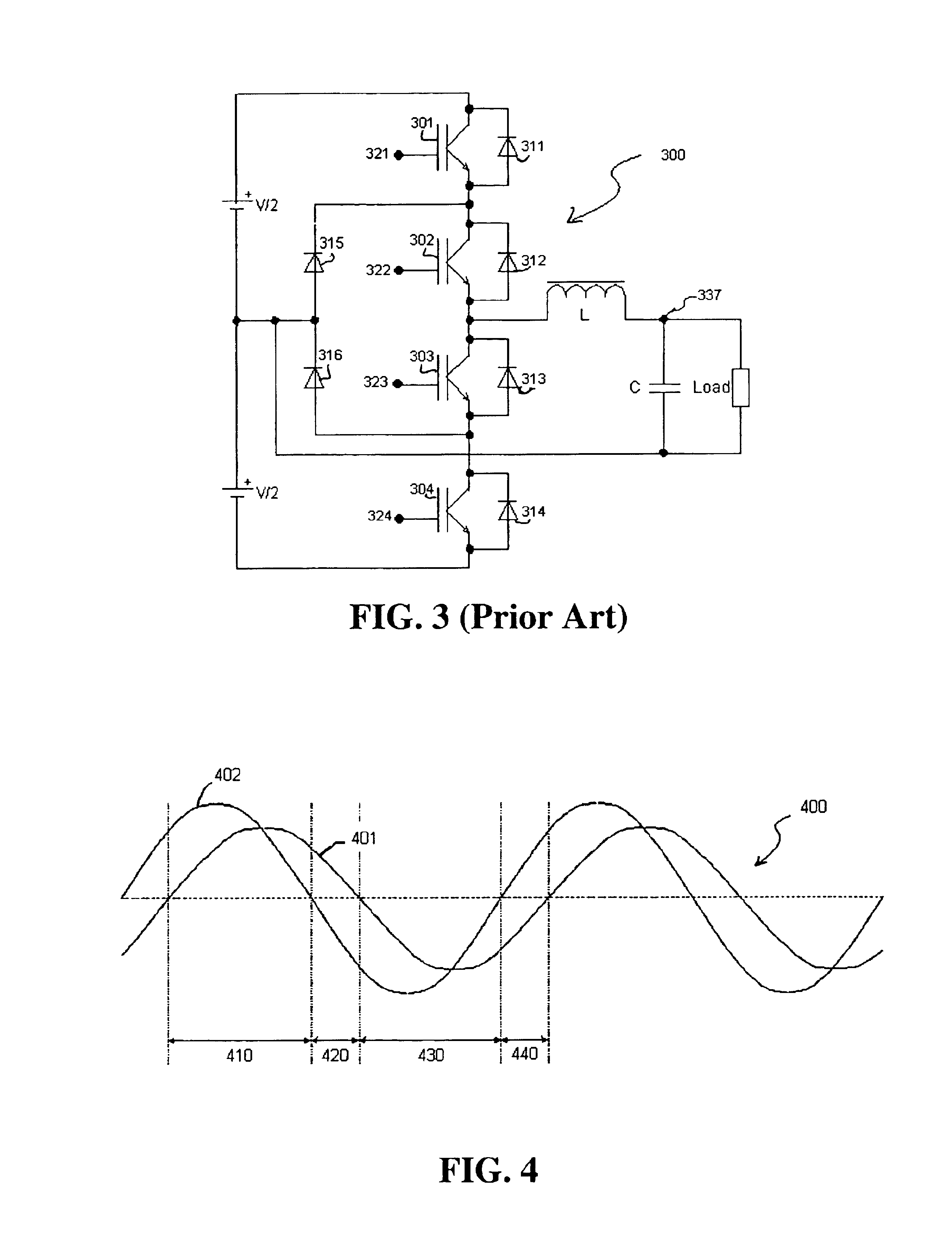
class="d_n">[0021]FIG. 7 is a comparison of prior art control signals and control signals used by the inverter of FIG. 6; and

[0022]FIG. 8 is a graphical comparison the ripple current through the output filter choke and voltage at the output of the filter stage used by the inverter of FIG. 6.

[0023]FIG. 9 is a plot of zero crossing distortion from certain control signals of FIG. 7.

[0024]FIG. 10 is a schematic of alternative embodiment control signals.

DETAILED DESCRIPTION OF THE INVENTION

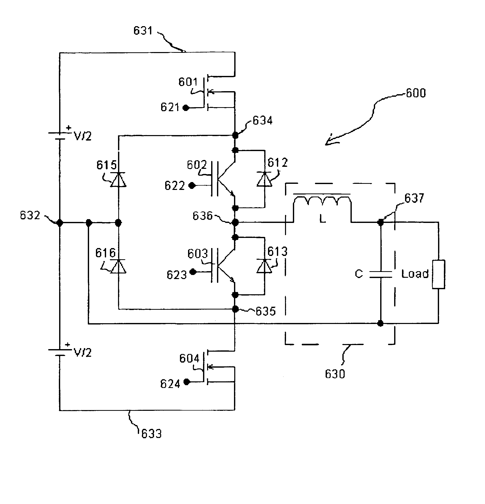
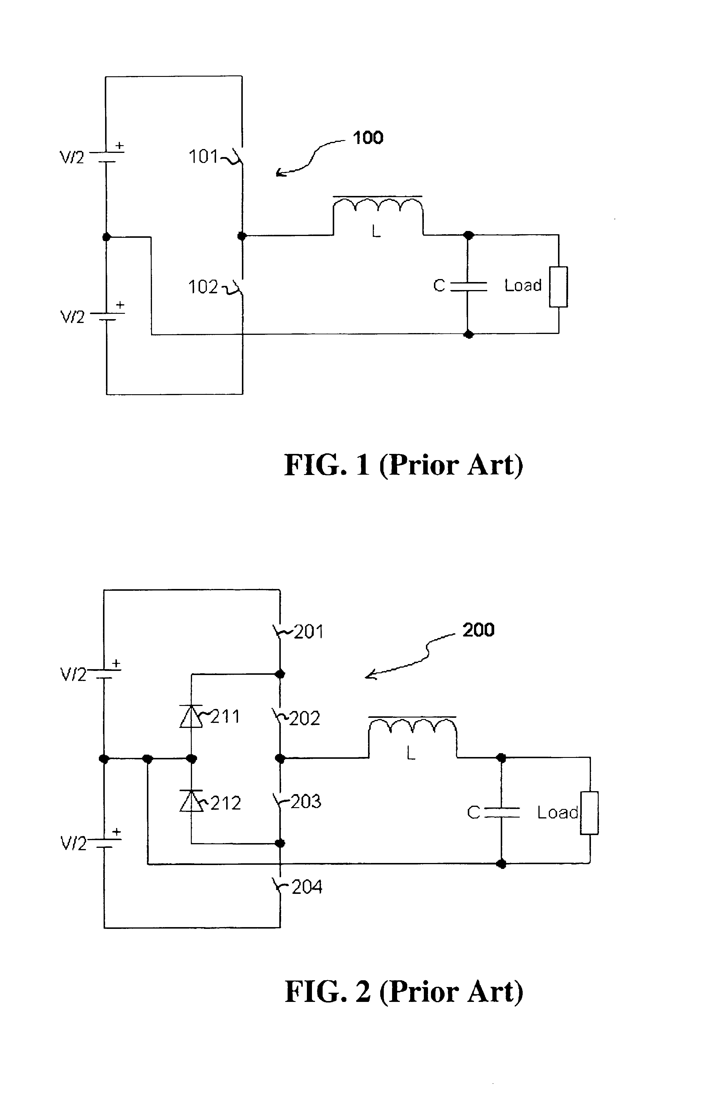
[0025]The invention relates to systems and methods for generating a three-level electrical output.

[0026]FIG. 5 shows an embodiment of the invention directed to an offline uninterruptible power supply (UPS) 500. The UPS 500 includes an input filter / surge protector 12, a transfer switch 14, a controller 16, a battery 18, a battery charger 19, an inverter 600, and a DC-DC converter 23. The UPS also includes an input 24 for coupling to an AC power source and an outlet 26 for coupling to a load.

[0027]The UP...


PUM


Abstract

The present invention relates to a high efficiency three-level inverter apparatus containing both bipolar and field effect transistors. An embodiment of a modified control scheme is also presented whereby transistors are modulated differently for each quadrant of output voltage-current phase. This embodiment of a modified control scheme allows efficient switching of field effect transistors without additional freewheeling and series diodes.

Description

FIELD OF THE INVENTION[0002]The invention relates at least in part to three-level inverters and pulse width modulation methods for efficient DC to AC conversion. More specifically, embodiments are further directed to three-level inverters and methods of power inversion for use in uninterruptible power supplies.BACKGROUND OF THE INVENTION[0003]PWM (Pulse Width Modulation) inverters are commonly used to convert DC power into AC power. Typical applications of these inverters include use in uninterruptible power supplies (UPS), fuel cells, photovoltaic panels, and wind turbines. Further, PWM inverters may be used to provide compensation for reactive loads, harmonic cancellation of supply grids, or as variable-speed drives for induction motors. The most commonly used inverters are two-level inverters and three-level inverters.[0004]Two-level inverters produce a modulated output having two fixed voltage levels. While potentially low cost, there are some drawbacks associated with using two...

Claims


Application Information

Patent Timeline
Patent Type & Authority Patents(United States)
IPC IPC(8): H02M7/48H02M7/483
CPCH02M7/487H02M1/0095
Inventor NIELSEN, HENNING ROAR
Owner AMERICA POWER CONVERSION CORP
Why Eureka
Try Eureka